
Datasheet

RL78/G12 1. OUTLINE
R01DS0193EJ0200 Rev.2.00
Sep 06, 2013
Page 13 of 106
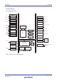
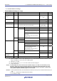
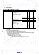
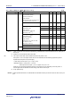
1.6.3 30-pin products
4
2
8
6
2
6
2
2
2
2
VOLTAGE
REGULATOR
REGC
ANI0/AV
REFP
ANI1/AV
REFM
ANI2, ANI3,
ANI16 to ANI19
TAU (8ch)
TI00
TO00
RxD0
TxD0
RxD2
TxD2
TOOL0
IICA0
On-chip debug
BCD adjustment
SCLA0
SDAA0
SCL20
SDA20
SCK20
SI20
SO20
SCL00
SDA00
SCL11
SDA11
RxD1
TxD1
SCK00
SI00
SO00
SCK11
SI11
SO11
TI01/TO01
TI02/TO02
TI03/TO03
(TI04/TO04)
(TI05/TO05)
(TI06/TO06)
(TI07/TO07)
ch0
ch1
ch2
ch3
ch4
ch5
ch6
ch7
SAU0 (4ch)
SAU0 (2ch)
Note
UART2
CSI20
IIC20
UART0
UART1
Note
CSI00
CSI11
Note
IIC00
Note
IIC11
Note
Low Speed
On-chip
oscillator
15 KHz
P00, P01
P10 to P17
P20 to P23
P30, P31
P40
P50, P51
P60, P61
P120
P121, P122
P137
P147
PCLBUZ0, PCLBUZ1
INTP0 to INTP5
Port 1
Port 0
Port 2
Port 3
Port 4
Port 5
Port 6
Port 12
Port 13
Port 14
Multiplier &
divider/
multiply-
accumulator
Code flash: 16 KB
Data flash: 2 KB
Note
Interrupt control
RL78
CPU
core
DMA
Note
2ch
RAM
2 KB
Poer-on
reset/voltage
detector
High-Speed
On-chip
oscillator
1 to 24 MHz
Clock Generator
+
Reset Generator
V
DD
V
SS
RESET
Main OSC
1 to 20 MHz
X1 X2/EXCLK
TOOL
TxD
TOOL
RxD
10-bit
A/D converter
8ch
12-bit Interval timer
Window watchdog
timer
CRC
Note
Interrupt control
6ch
Buzzer/clock
output control
Note Provided only in the R5F102 products.
Remark Functions in parentheses in the above figure can be assigned via settings in the peripheral I/O redirection
register (PIOR). See Figure 4-8 Format of Peripheral I/O Redirection Register (PIOR) in the RL78/G12
User’s Manual Hardware.