
Datasheet

RL78/G12 3. ELECTRICAL SPECIFICATIONS (G: T
A = −40 to +105°C)
R01DS0193EJ0200 Rev.2.00
Sep 06, 2013
Page 97 of 106
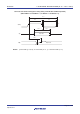
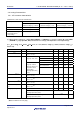
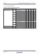
(3) When reference voltage (+) = VDD (ADREFP1 = 0, ADREFP0 = 0), reference voltage (−) = VSS (ADREFM = 0),
target pin: ANI0 to ANI3, ANI16 to ANI22, internal reference voltage, and temperature sensor output voltage
(T
A = −40 to +105°C, 2.4 V ≤ VDD ≤ 5.5 V, VSS = 0 V, Reference voltage (+) = VDD, Reference voltage (−) = VSS)
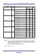
Parameter Symbol Conditions MIN. TYP. MAX. Unit
Resolution RES 8 10 bit
Overall error
Note 1
AINL 10-bit resolution 1.2 ±7.0 LSB
Conversion time tCONV
10-bit resolution
Target pin: ANI0 to ANI3,
ANI16 to ANI22
3.6 V ≤ VDD ≤ 5.5 V 2.125 39
μ
s
2.7 V ≤ VDD ≤ 5.5 V 3.1875 39
μ
s
2.4 V ≤ VDD ≤ 5.5 V 17 39
μ
s
Conversion time tCONV
10-bit resolution
Target pin: internal reference
voltage, and temperature
sensor output voltage (HS
(high-speed main) mode)
3.6 V ≤ VDD ≤ 5.5 V 2.375 39
μ
s
2.7 V ≤ VDD ≤ 5.5 V 3.5625 39
μ
s
2.4 V ≤ VDD ≤ 5.5 V 17 39
μ
s
Zero-scale error
Notes 1, 2
EZS 10-bit resolution ±0.60 %FSR
Full-scale error
Notes 1, 2
EFS 10-bit resolution ±0.60 %FSR
Integral linearity error
Note 1
ILE 10-bit resolution ±4.0 LSB
Differential linearity error
Note 1
DLE 10-bit resolution ±2.0 LSB
Analog input voltage VAIN ANI0 to ANI3, ANI16 to ANI22 0 VDD V
Internal reference voltage
(HS (high-speed main) mode)
V
BGR
Note 3
V
Temperature sensor output voltage
(HS (high-speed main) mode)
V
TMPS25
Note 3
V
Notes 1. Excludes quantization error (±1/2 LSB).
2. This value is indicated as a ratio (%FSR) to the full-scale value.
3. Refer to 3.6.2 Temperature sensor/internal reference voltage characteristics.