
Datasheet

RL78/G12 3. ELECTRICAL SPECIFICATIONS (G: T
A = −40 to +105°C)
R01DS0193EJ0200 Rev.2.00
Sep 06, 2013
Page 71 of 106
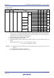
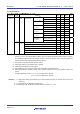
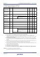
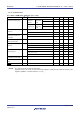
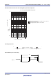
(2) 30-pin products
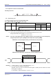
(TA = −40 to +105°C, 2.4 V ≤ VDD ≤ 5.5 V, VSS = 0 V) (1/2)
Parameter Symbol Conditions MIN. TYP. MAX. Unit
Supply
current
Note 1
I
DD1
Operating
mode
HS (High-speed
main) mode
Note 4
f
IH
= 24 MHz
Note 3
Basic
operation
VDD = 5.0 V 1.5 mA
VDD = 3.0 V 1.5
Normal
operation
VDD = 5.0 V 3.7 5.8 mA
VDD = 3.0 V 3.7 5.8
f
IH
= 16 MHz
Note 3
VDD = 5.0 V 2.7 4.2 mA
VDD = 3.0 V 2.7 4.2
f
MX
= 20 MHz
Note 2
,
V
DD
= 5.0 V
Square wave input 3.0 4.9 mA
Resonator connection 3.2 5.0
f
MX
= 20 MHz
Note 2
,
V
DD
= 3.0 V
Square wave input 3.0 4.9 mA
Resonator connection 3.2 5.0
f
MX
= 10 MHz
Note 2
,
V
DD
= 5.0 V
Square wave input 1.9 2.9 mA
Resonator connection 1.9 2.9
f
MX
= 10 MHz
Note 2
,
V
DD
= 3.0 V
Square wave input 1.9 2.9 mA
Resonator connection 1.9 2.9
Notes 1. Total current flowing into VDD, including the input leakage current flowing when the level of the input pin is
fixed to V
DD or VSS. The values below the MAX. column include the peripheral operation current. However,
not including the current flowing into the A/D converter, LVD circuit, I/O port, and on-chip pull-up/pull-down
resistors and the current flowing during data flash rewrite.
2. When high-speed on-chip oscillator clock is stopped.
3. When high-speed system clock is stopped
4. Relationship between operation voltage width, operation frequency of CPU and operation mode is as
follows.
HS(High speed main) mode: V
DD = 2.7 V to 5.5 V @1 MHz to 24 MHz
V
DD = 2.4 V to 5.5 V @1 MHz to 16 MHz
Remarks 1. f
MX: High-speed system clock frequency (X1 clock oscillation frequency or external main system clock
frequency)
2. f
IH: high-speed on-chip oscillator clock frequency
3. Temperature condition of the TYP. value is T
A = 25°C.