
Datasheet

RL78/G12 3. ELECTRICAL SPECIFICATIONS (G: T
A = −40 to +105°C)
R01DS0193EJ0200 Rev.2.00
Sep 06, 2013
Page 68 of 106
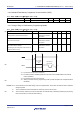
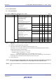
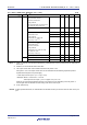
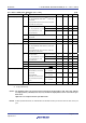
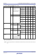
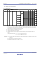
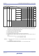
(TA = −40 to +105°C, 2.4 V ≤ VDD ≤ 5.5 V, VSS = 0 V) (4/4)
Parameter Symbol Conditions MIN. TYP. MAX. Unit
Output voltage, low VOL1
20-, 24-pin products:
P00 to P03
Note
, P10 to P14,
P40 to P42
30-pin products: P00, P01,
P10 to P17, P30, P31, P40,
P50, P51, P120, P147
4.0 V ≤ V
DD ≤ 5.5 V,
I
OL1 = 8.5 mA
0.7 V
2.7 V ≤ VDD ≤ 5.5 V,
I
OL1 = 3.0 mA
0.6 V
2.7 V ≤ VDD ≤ 5.5 V,
I
OL1 = 1.5 mA
0.4 V
2.4 V ≤ VDD ≤ 5.5 V,
I
OL1 = 0.6 mA
0.4 V
VOL2 P20 to P23 IOL2 = 400
μ
A 0.4 V
VOL3 P60, P61
4.0 V ≤ V
DD ≤ 5.5 V,
I
OL1 = 15.0 mA
2.0 V
4.0 V ≤ VDD ≤ 5.5 V,
I
OL1 = 5.0 mA
0.4 V
2.7 V ≤ VDD ≤ 5.5 V,
I
OL1 = 3.0 mA
0.4 V
2.4 V ≤ VDD ≤ 5.5 V,
I
OL1 = 2.0 mA
0.4 V
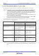
Input leakage current,
high
I
LIH1
Other than P121,
P122
VI = VDD 1
μ
A
ILIH2
P121, P122
(X1, X2/EXCLK)
V
I = VDD
Input port or external
clock input
1
μ
A
When resonator
connected
10
μ
A
Input leakage current,
low
I
LIL1
Other than P121,
P122
VI = VSS −1
μ
A
ILIL2
P121, P122
(X1, X2/EXCLK)
V
I = VSS
Input port or external
clock input
−1
μ
A
When resonator
connected
−10
μ
A
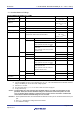
On-chip pull-up
resistance
R
U
20-, 24-pin products:
P00 to P03
Note
, P10 to P14,
P40 to P42, P125, RESET
30-pin products: P00, P01,
P10 to P17, P30, P31, P40,
P50, P51, P120, P147
V
I = VSS, input port 10 20 100 kΩ
Note 24-pin products only.
Remark Unless specified otherwise, the characteristics of alternate-function pins are the same as those of the port
pins.