
Datasheet


RL78/G12 2. ELECTRICAL SPECIFICATIONS (A, D: T
A = −40 to +85°C)
R01DS0193EJ0200 Rev.2.00
Sep 06, 2013
Page 48 of 106
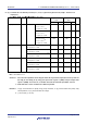
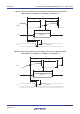
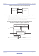
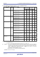
CSI mode connection diagram (during communication at different potential)
RL78
microcontroller
SOp
SCK
SI
User's device
SIp
SO
V
b
R
b
SCKp
<Slave>
Remarks 1. Rb [Ω]: Communication line (SOp) pull-up resistance, Cb [F]: Communication line (SOp) load capacitance,
V
b [V]: Communication line voltage
2. p: CSI number (p = 00, 20), m: Unit number (m = 0, 1), n: Channel number (n = 0)
3. fMCK: Serial array unit operation clock frequency
(Operation clock to be set by the serial clock select register m (SPSm) and the CKSmn bit of serial mode
register mn (SMRmn). m: Unit number, n: Channel number (mn = 00, 10))
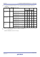
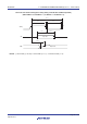
CSI mode serial transfer timing (slave mode) (during communication at different potential)
(When DAPmn = 0 and CKPmn = 0, or DAPmn = 1 and CKPmn = 1.)
t
KCY2
t
KL2
t
KH2
t
SIK2
t
KSI2
t
KSO2
SIp
SOp
SCKp
Input data
Output data