
Datasheet


RL78/G12 2. ELECTRICAL SPECIFICATIONS (A, D: T
A = −40 to +85°C)
R01DS0193EJ0200 Rev.2.00
Sep 06, 2013
Page 45 of 106
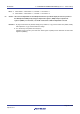
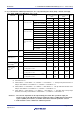
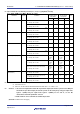
(8) Communication at different potential (1.8 V, 2.5 V, 3 V) (CSI mode) (master mode, SCKp... internal clock
output) (3/3)
(TA = −40 to +85°C, 1.8 V ≤ VDD ≤ 5.5 V, VSS = 0 V)
Parameter Symbol Conditions
HS (high-speed
main) Mode
LS (low-speed
main) Mode
Unit
MIN. MAX. MIN. MAX.
SIp setup time
(to SCKp↓)
Note 1
t
SIK1
4.0 V ≤ V
DD ≤ 5.5 V, 2.7 V ≤ Vb ≤ 4.0 V,
C
b = 30 pF, Rb = 1.4 kΩ
44
110
ns
2.7 V ≤ VDD < 4.0 V, 2.3 V ≤ Vb ≤ 2.7 V,
C
b = 30 pF, Rb = 2.7 kΩ
44
110
ns
1.8 V ≤ VDD < 3.3 V, 1.6 V ≤ Vb ≤ 2.0 V
Note 2
,
C
b = 30 pF, Rb = 5.5 kΩ
110
110
ns
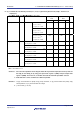
SIp hold time
(from SCKp↓)
Note 1
t
KSI1
4.0 V ≤ V
DD ≤ 5.5 V, 2.7 V ≤ Vb ≤ 4.0 V,
C
b = 30 pF, Rb = 1.4 kΩ
19 19 ns
2.7 V ≤ VDD < 4.0 V, 2.3 V ≤ Vb ≤ 2.7 V,
C
b = 30 pF, Rb = 2.7 kΩ
19 19 ns
1.8 V ≤ VDD < 3.3 V, 1.6 V ≤ Vb ≤ 2.0 V
Note 2
,
C
b = 30 pF, Rb = 5.5 kΩ
19 19 ns
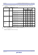
Delay time from
SCKp↑ to
SOp output
Note 1
t
KSO1
4.0 V ≤ V
DD ≤ 5.5 V, 2.7 V ≤ Vb ≤ 4.0 V,
C
b = 30 pF, Rb = 1.4 kΩ
25 25 ns
2.7 V ≤ VDD < 4.0 V, 2.3 V ≤ Vb ≤ 2.7 V,
C
b = 30 pF, Rb = 2.7 kΩ
25 25 ns
1.8 V ≤ VDD < 3.3 V, 1.6 V ≤ Vb ≤ 2.0 V
Note 2
,
C
b = 30 pF, Rb = 5.5 kΩ
25 25 ns
Notes 1. When DAPmn = 0 and CKPmn = 1, or DAPmn = 1 and CKPmn = 0.
2. Use it with V
DD ≥ Vb.
Cautions 1. Select the TTL input buffer for the SIp pin and the N-ch open drain output (V
DD tolerance) mode
for the SOp pin and SCKp pin by using port input mode register 1 (PIM1) and port output mode
register 1 (POM1). For V
IH and VIL, see the DC characteristics with TTL input buffer selected.
2. CSI01 and CSI11 cannot communicate at different potential.
Remarks 1. R
b [Ω]: Communication line (SCKp, SOp) pull-up resistance, Cb [F]: Communication line (SCKp, SOp)
load capacitance, V
b [V]: Communication line voltage
2. p: CSI number (p = 00, 20), m: Unit number (m = 0, 1), n: Channel number (n = 0)
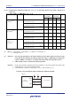
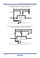
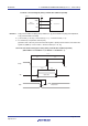
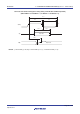
CSI mode connection diagram (during communication at different potential)
Vb
Rb
SCKp
SOp
SCK
SI
User's device
SIp
SO
V
b
Rb
<Master>
RL78
microcontroller
<R>
<R>
<R>