
Datasheet

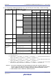

RL78/G12 2. ELECTRICAL SPECIFICATIONS (A, D: T
A = −40 to +85°C)
R01DS0193EJ0200 Rev.2.00
Sep 06, 2013
Page 42 of 106
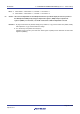
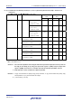
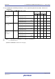
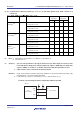
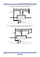
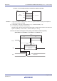
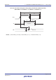
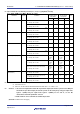
Notes 1. When DAP00 = 0 and CKP00 = 0, or DAP00 = 1 and CKP00 = 1
2. When DAP00 = 0 and CKP00 = 1, or DAP00 = 1 and CKP00 = 0.
Caution Select the TTL input buffer for the SI00 pin and the N-ch open drain output (V
DD tolerance) mode for
the SO00 pin and SCK00 pin by using port input mode register 1 (PIM1) and port output mode
register 1 (POM1). For V
IH and VIL, see the DC characteristics with TTL input buffer selected.
Remarks 1. R
b [Ω]:Communication line (SCK00, SO00) pull-up resistance, Cb [F]: Communication line (SCK00, SO00)
load capacitance, Vb [V]: Communication line voltage
2. f
MCK: Serial array unit operation clock frequency
(Operation clock to be set by the serial clock select register 0 (SPS0) and the CKS00 bit of serial mode
register 00 (SMR00).)
<R>