
Datasheet

RL78/G12 2. ELECTRICAL SPECIFICATIONS (A, D: T
A = −40 to +85°C)
R01DS0193EJ0200 Rev.2.00
Sep 06, 2013
Page 36 of 106
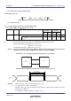
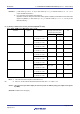
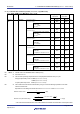
Remarks 1. p: CSI number (p = 00, 01, 11, 20), m: Unit number (m = 0, 1), n: Channel number (n = 0, 1, 3: “1, 3” is
only for the R5F102 products.)
2. f
MCK: Serial array unit operation clock frequency
(Operation clock to be set by the serial clock select register m (SPSm) and the CKSmn bit of serial mode
register mn (SMRmn). m: Unit number (m = 0, 1), n: Channel number (n = 0, 1, 3: “1, 3” is only for the
R5F102 products.))
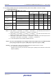
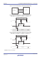
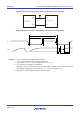
(5) During communication at same potential (simplified I
2
C mode)
(TA = −40 to +85°C, 1.8 V ≤ VDD ≤ 5.5 V, VSS = 0 V)
Parameter Symbol Conditions HS (high-speed main) Mode
LS (low-speed main) Mode
Unit
MIN. MAX.
SCLr clock frequency fSCL 1.8 V ≤ VDD ≤ 5.5 V,
C
b = 100 pF, Rb = 3 kΩ
400
Note 1
kHz
1.8 V ≤ VDD < 2.7 V,
C
b = 100 pF, Rb = 5 kΩ
300
Note 1
kHz
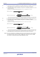
Hold time when SCLr = “L” tLOW 1.8 V ≤ VDD ≤ 5.5 V,
C
b = 100 pF, Rb = 3 kΩ
1150 ns
1.8 V ≤ VDD < 2.7 V,
C
b = 100 pF, Rb = 5 kΩ
1550 ns
Hold time when SCLr = “H” tHIGH 1.8 V ≤ VDD ≤ 5.5 V,
C
b = 100 pF, Rb = 3 kΩ
1150 ns
1.8 V ≤ VDD < 2.7 V,
C
b = 100 pF, Rb = 5 kΩ
1550 ns
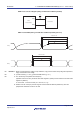
Data setup time (reception) tSU:DAT 1.8 V ≤ VDD ≤ 5.5 V,
C
b = 100 pF, Rb = 3 kΩ
1/f
MCK + 145
Note
2
ns
1.8 V ≤ VDD < 2.7 V,
C
b = 100 pF, Rb = 5 kΩ
1/f
MCK + 230
Note
2
ns
Data hold time (transmission) tHD:DAT 1.8 V ≤ VDD ≤ 5.5 V,
C
b = 100 pF, Rb = 3 kΩ
0 355 ns
1.8 V ≤ VDD < 2.7 V,
C
b = 100 pF, Rb = 5 kΩ
0 405 ns
Notes 1. The value must also be equal to or less than f
MCK/4.
2. Set t
SU:DAT so that it will not exceed the hold time when SCLr = "L" or SCLr = "H".
Caution Select the N-ch open drain output (V
DD tolerance) mode for SDAr by using port output mode register
h (POMh).
(Remarks are listed on the next page.)
<R>
<R>