
Datasheet

RL78/G12 2. ELECTRICAL SPECIFICATIONS (A, D: T
A = −40 to +85°C)
R01DS0193EJ0200 Rev.2.00
Sep 06, 2013
Page 34 of 106
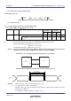
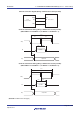
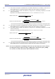
(4) During communication at same potential (CSI mode) (slave mode, SCKp... external clock input)
(TA = −40 to +85°C, 1.8 V ≤ VDD ≤ 5.5 V, VSS = 0 V)
Parameter Symbol Conditions
HS (high-speed
main) Mode
LS (low-speed main)
Mode
Unit
MIN. MAX. MIN. MAX.
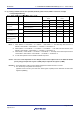
SCKp cycle time
Note4
tKCY2 4.0 V ≤ VDD ≤ 5.5 V 20 MHz < fMCK 8/fMCK
−
ns
fMCK ≤ 20 MHz 6/fMCK 6/fMCK ns
2.7 V ≤ VDD ≤ 5.5 V 16 MHz < fMCK 8/fMCK
−
ns
fMCK ≤ 16 MHz 6/fMCK 6/fMCK ns
2.4 V ≤ VDD ≤ 5.5 V 6/fMCK
and 500
6/f
MCK
and 500
ns
1.8 V ≤ VDD ≤ 5.5 V
−
6/fMCK
and 750
ns
SCKp high-/low-level
width
t
KH2,
t
KL2
4.0 V ≤ V
DD ≤ 5.5 V tKCY2/2−7 tKCY2/2−7 ns
2.7 V ≤ VDD ≤ 5.5 V tKCY2/2−8 tKCY2/2−8 ns
2.4 V ≤ VDD ≤ 5.5 V tKCY2/2−18 tKCY2/2−18 ns
1.8 V ≤ VDD ≤ 5.5 V
−
tKCY2/2−18 ns
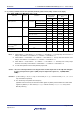
SIp setup time
(to SCKp↑)
Note 1
t
SIK2 2.7 V ≤ VDD ≤ 5.5 V
1/f
MCK +
20
1/f
MCK +
30
ns
2.4 V ≤ VDD ≤ 5.5 V
1/f
MCK +
30
1/f
MCK +
30
ns
1.8 V ≤ VDD ≤ 5.5 V
−
1/f
MCK +
30
ns
SIp hold time
(from SCKp↑)
Note 2
t
KSI2
1/f
MCK +
31
1/f
MCK +
31
ns
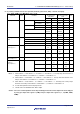
Delay time from
SCKp↓ to
SOp output
Note 3
t
KSO2 C = 30 pF
Note4
2.7 V ≤ VDD ≤ 5.5 V
2/f
MCK +
44
2/f
MCK +
110
ns
2.4 V ≤ VDD ≤ 5.5 V
2/f
MCK +
75
2/fMCK +
110
ns
1.8 V ≤ VDD ≤ 5.5 V
−
2/f
MCK +
110
ns
Notes 1. When DAPmn = 0 and CKPmn = 0, or DAPmn = 1 and CKPmn = 1. The SIp setup time becomes “to
SCKp↓” when DAPmn = 0 and CKPmn = 1, or DAPmn = 1 and CKPmn = 0.
2. When DAPmn = 0 and CKPmn = 0, or DAPmn = 1 and CKPmn = 1. The SIp hold time becomes “from
SCKp↓” when DAPmn = 0 and CKPmn = 1, or DAPmn = 1 and CKPmn = 0.
3. When DAPmn = 0 and CKPmn = 0, or DAPmn = 1 and CKPmn = 1. The delay time to SOp output
becomes “from SCKp↑” when DAPmn = 0 and CKPmn = 1, or DAPmn = 1 and CKPmn = 0.
4. C is the load capacitance of the SOp output lines.
5. Transfer rate in the SNOOZE mode: MAX. 1 Mbps
Caution Select the normal input buffer for the SIp and SCKp pins and the normal output mode for the SOp pin
by using port input mode register 1 (PIM1) and port output mode registers 0, 1, 4 (POM0, POM1,
POM4).
<R>