
Datasheet


RL78/G12 1. OUTLINE
R01DS0193EJ0200 Rev.2.00
Sep 06, 2013
Page 14 of 106
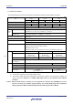
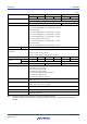
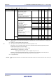
1.7 Outline of Functions
This outline describes the function at the time when Peripheral I/O redirection register (PIOR) is set to 00H.
(1/2)
Item 20-pin 24-pin 30-pin
R5F1026x R5F1036x R5F1027x R5F1037x R5F102Ax R5F103Ax
Code flash memory 2 to 16 KB
Note 1
4 to 16 KB
Data flash memory 2 KB
−
2 KB
−
2 KB
−
RAM 256 B to 1.5 KB 512 B to 1.5 KB 512 B to 2KB
Address space 1 MB
Main
system
clock
High-speed system clock
X1, X2 (crystal/ceramic) oscillation, external main system clock input (EXCLK)
1 to 20 MHz: V
DD = 2.7 to 5.5 V, 1 to 8 MHz: VDD = 1.8 to 5.5 V
High-speed on-chip
oscillator clock
HS (High-speed main) mode : 1 to 24 MHz (VDD = 2.7 to 5.5 V), 1 to 16 MHz (VDD = 2.4 to 5.5 V),
LS (Low-speed main) mode : 1 to 8 MHz (V
DD = 1.8 to 5.5 V)
Low-speed on-chip oscillator clock 15 kHz (TYP)
General-purpose register (8-bit register × 8) × 4 banks
Minimum instruction execution time 0.04167
μ
s (High-speed on-chip oscillator clock: fIH = 24 MHz operation)
0.05
μ
s (High-speed system clock: fMX = 20 MHz operation)
Instruction set Data transfer (8/16 bits)
Adder and subtractor/logical operation (8/16 bits)
Multiplication (8 bits × 8 bits)
Rotate, barrel shift, and bit manipulation (set, reset, test, and Boolean operation), etc.
I/O port Total 18 22 26
CMOS I/O
12
(N-ch O.D. I/O
[V
DD withstand voltage]: 4)
16
(N-ch O.D. I/O
[VDD withstand voltage]: 5)
21
(N-ch O.D. I/O
[VDD withstand voltage]: 9)
CMOS input 4 4 3
N-ch open-drain I/O
(6 V tolerance)
2
Timer 16-bit timer 4 channels 8 channels
Watchdog timer 1 channel
12-bit Interval timer 1 channel
Timer output
4 channels
(PWM outputs: 3
Note 3
)
8 channels
(PWM outputs: 7
Note 3
)
Note 2
Notes 1. The self-programming function cannot be used in the R5F10266 and R5F10366.
2. The maximum number of channels when PIOR0 is set to 1.
3. The number of PWM outputs varies depending on the setting of channels in use (the number of masters and
slaves). (See 6.9.3 Operation as multiple PWM output function in the RL78/G12 User’s Manual
Hardware.)
Caution When the flash memory is rewritten via a user program, the code flash area and RAM area are used
because each library is used. When using the library, refer to RL78 Family Flash Self Programming
Library Type01 User's Manual and RL78 Family Data Flash Library Type04 User's Manual.
<R>