
Datasheet

C - 1
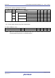
Revision History RL78/G12 Data Sheet
Description
Rev. Date
Page Summary
1.00 Dec 10, 2012 - First Edition issued
1 Modification of 1.1 Features
3 Modification of 1.2 List of Part Numbers
4 Modification of Table 1-1. List of Ordering Part Numbers, Note, and Caution
7 to 9 Modification of package name in 1.4.1 to 1.4.3
14 Modification of tables in 1.7 Outline of Functions
17 Modification of description of table in 2.1 Absolute Maximum Ratings (TA = 25°C)
18 Modification of table, Note, and Caution in 2.2.1 X1 oscillator characteristics
18 Modification of table in 2.2.2 On-chip oscillator characteristics
19
Modification of Note 3 in 2.3.1 Pin characteristics (1/4)
20
Modification of Note 3 in 2.3.1 Pin characteristics (2/4)
23
Modification of Notes 1 and 2 in (1) 20-, 24-pin products (1/2)
24
Modification of Notes 1 and 3 in (1) 20-, 24-pin products (2/2)
25
Modification of Notes 1 and 2 in (2) 30-pin products (1/2)
26
Modification of Notes 1 and 3 in (2) 30-pin products (2/2)
27
Modification of (3) Peripheral functions (Common to all products)
28
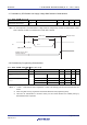
Modification of table in 2.4 AC Characteristics
29
Addition of Minimum Instruction Execution Time during Main System Clock Operation
30
Modification of figures of AC Timing Test Point and External Main System Clock Timing
31
Modification of figure of AC Timing Test Point
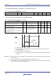
31
Modification of description and Note 2 in (1) During communication at same
potential (UART mode)
32
Modification of description in (2) During communication at same potential (CSI mode)
33
Modification of description in (3) During communication at same potential (CSI mode)
34
Modification of description in (4) During communication at same potential (CSI mode)
36
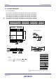
Modification of table and Note 2 in (5) During communication at same potential
(simplified I
2
C mode)
38, 39
Modification of table and Notes 1 to 9 in (6) Communication at different potential
(1.8 V, 2.5 V, 3 V) (UART mode)
40
Modification of Remarks 1 to 3 in (6) Communication at different potential (1.8 V,
2.5 V, 3 V) (UART mode)
41
Modification of table in (7) Communication at different potential (2.5 V, 3 V) (CSI mode)
42
Modification of Caution in (7) Communication at different potential (2.5 V, 3 V) (CSI mode)
43
Modification of table in (8) Communication at different potential (1.8 V, 2.5 V, 3 V)
(CSI mode) (1/3)
44
Modification of table and Notes 1 and 2 in (8) Communication at different potential
(1.8 V, 2.5 V, 3 V) (CSI mode) (2/3)
45
Modification of table, Note 1, and Caution 1 in (8) Communication at different
potential (1.8 V, 2.5 V, 3 V) (CSI mode) (3/3)
47
Modification of table in (9) Communication at different potential (1.8 V, 2.5 V, 3 V)
(CSI mode)
50
Modification of table, Note 1, and Caution 1 in (10) Communication at different
potential (1.8 V, 2.5 V, 3 V) (simplified I
2
C mode)
52
Modification of Remark in 2.5.2 Serial interface IICA
53
Addition of table to 2.6.1 A/D converter characteristics
53
Modification of description in 2.6.1 (1)
54
Modification of Notes 3 to 5 in 2.6.1 (1)
2.00 Sep 06, 2013
54
Modification of description and Notes 2 to 4 in 2.6.1 (2)