
Datasheet


RL78/G12 1. OUTLINE
R01DS0193EJ0200 Rev.2.00
Sep 06, 2013
Page 10 of 106
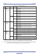
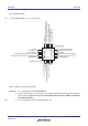
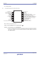
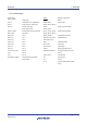
1.5 Pin Identification
A
NI0 to ANI3,
A
NI16 to ANI22:
A
nalog input
REGC:
RESET:
Regulator Capacitance
Reset
A
VREFM:
A
nalog Reference Voltage Minus RxD0 to RxD2:
SCK00, SCK01, SCK11,
Receive Data
A
VREFP:
A
nalog reference voltage plus
EXCLK: External Clock Input
(Main System Clock)
SCK20:
SCL00, SCL01,
Serial Clock Input/Output
INTP0 to INTP5 Interrupt Request From Peripheral SCL11, SCL20, SCLA0:
SDA00, SDA01, SDA11,
Serial Clock Input/Output
KR0 to KR9: Key Return
P00 to P03: Port 0 SDA20, SDAA0: Serial Data Input/Output
P10 to P17: Port 1 SI00, SI01, SI11, SI20: Serial Data Input
P20 to P23: Port 2 SO00, SO01, SO11,
P30 to P31: Port 3 SO20: Serial Data Output
P40 to P42: Port 4 TI00 to TI07: Timer Input
P50, P51: Port 5 TO00 to TO07: Timer Output
P60, P61: Port 6 TOOL0: Data Input/Output for Tool
P120 to P122, P125: Port 12 TOOLRxD, TOOLTxD: Data Input/Output for External
Device P137: Port 13
P147: Port 14 TxD0 to TxD2: Transmit Data
PCLBUZ0, PCLBUZ1: Programmable Clock Output/
Buzzer Output
V
DD: Power supply
V
SS: Ground
X1, X2:
Crystal Oscillator (Main System
Clock)