
Datasheet

RL78/G13 3. ELECTRICAL SPECIFICATIONS (G: T
A = -40 to +105°C)
Page 161 of 194R01DS0131EJ0310 Rev.3.10
Nov 15, 2013
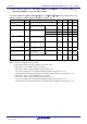
Notes 1. Transfer rate in the SNOOZE mode : MAX. 1 Mbps
2. When DAPmn = 0 and CKPmn = 0, or DAPmn = 1 and CKPmn = 1. The SIp setup time becomes “to
SCKp↓” when DAPmn = 0 and CKPmn = 1, or DAPmn = 1 and CKPmn = 0.
3. When DAPmn = 0 and CKPmn = 0, or DAPmn = 1 and CKPmn = 1. The SIp hold time becomes “from
SCKp↓” when DAPmn = 0 and CKPmn = 1, or DAPmn = 1 and CKPmn = 0.
4. When DAPmn = 0 and CKPmn = 0, or DAPmn = 1 and CKPmn = 1. The delay time to SOp output
becomes “from SCKp↑” when DAPmn = 0 and CKPmn = 1, or DAPmn = 1 and CKPmn = 0.
Caution Select the TTL input buffer for the SIp pin and SCKp pin and the N-ch open drain output (VDD
tolerance (When 20- to 52-pin products)/EV
DD tolerance (When 64- to 128-pin products)) mode for
the SOp pin by using port input mode register g (PIMg) and port output mode register g (POMg).
For VIH and VIL, see the DC characteristics with TTL input buffer selected.
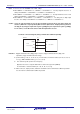
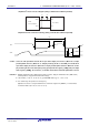
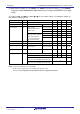
CSI mode connection diagram (during communication at different potential)
RL78
microcontroller
SCKp
<Slave>
SOp
SCK
SI
SIp
SO
V
b
R
b
User device
Remarks 1. R
b[Ω]:Communication line (SOp) pull-up resistance, Cb[F]: Communication line (SOp) load
capacitance, V
b[V]: Communication line voltage
2. p: CSI number (p = 00, 01, 10, 20, 30, 31), m: Unit number, n: Channel number (mn = 00, 01, 02, 10,
12, 13), g: PIM and POM number (g = 0, 1, 4, 5, 8, 14)
3. f
MCK: Serial array unit operation clock frequency
(Operation clock to be set by the CKSmn bit of serial mode register mn (SMRmn).
m: Unit number, n: Channel number (mn = 00, 01, 02, 10, 12, 13))
4. CSI01 of 48-, 52-, 64-pin products, and CSI11 and CSI21 cannot communicate at different potential.
Use other CSI for communication at different potential.