
Datasheet


RL78/G13 2. ELECTRICAL SPECIFICATIONS (A, D: T
A = -40 to +85°C)
Page 85 of 194R01DS0131EJ0310 Rev.3.10
Nov 15, 2013
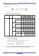
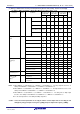
Remarks 1. p: CSI number (p = 00, 01, 10, 11, 20, 21, 30, 31), m: Unit number (m = 0, 1), n: Channel number (n = 0
to 3),
g: PIM and POM numbers (g = 0, 1, 4, 5, 8, 14)
2. f
MCK: Serial array unit operation clock frequency
(Operation clock to be set by the CKSmn bit of serial mode register mn (SMRmn). m: Unit number,
n: Channel number (mn = 00 to 03, 10 to 13))
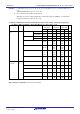
(4) During communication at same potential (CSI mode) (slave mode, SCKp... external clock input) (1/2)
(T
A = −40 to +85°C, 1.6 V ≤ EVDD0 = EVDD1 ≤ VDD ≤ 5.5 V, VSS = EVSS0 = EVSS1 = 0 V)
Parameter Symbol Conditions HS (high-speed
main) Mode
LS (low-speed
main) Mode
LV (low-voltage
main) Mode
Unit
MIN. MAX. MIN. MAX. MIN. MAX.
SCKp cycle time
Note 5
t
KCY2 4.0 V ≤ EVDD0 ≤ 5.5
V
20 MHz < fMCK 8/fMCK ⎯ ⎯ ns
fMCK ≤ 20 MHz 6/fMCK 6/fMCK 6/fMCK ns
2.7 V ≤ EVDD0 ≤ 5.5
V
16 MHz < fMCK 8/fMCK ⎯ ⎯ ns
fMCK ≤ 16 MHz 6/fMCK 6/fMCK 6/fMCK ns
2.4 V ≤ EVDD0 ≤ 5.5 V 6/fMCK
and 500
6/f
MCK
and
500
6/f
MCK
and
500
ns
1.8 V ≤ EVDD0 ≤ 5.5 V 6/fMCK
and 750
6/f
MCK
and
750
6/f
MCK
and
750
ns
1.7 V ≤ EVDD0 ≤ 5.5 V 6/fMCK
and
1500
6/f
MCK
and
1500
6/f
MCK
and
1500
ns
1.6 V ≤ EVDD0 ≤ 5.5 V ⎯ 6/fMCK
and
1500
6/f
MCK
and
1500
ns
SCKp high-/low-
level width
tKH2,
t
KL2
4.0 V ≤ EV
DD0 ≤ 5.5 V tKCY2/2 −
7
tKCY2/2
− 7
tKCY2/2
− 7
ns
2.7 V ≤ EVDD0 ≤ 5.5 V tKCY2/2 −
8
tKCY2/2
− 8
tKCY2/2
− 8
ns
1.8 V ≤ EVDD0 ≤ 5.5 V tKCY2/2 −
18
tKCY2/2
− 18
tKCY2/2
− 18
ns
1.7 V ≤ EVDD0 ≤ 5.5 V tKCY2/2 −
66
tKCY2/2
− 66
tKCY2/2
− 66
ns
1.6 V ≤ EVDD0 ≤ 5.5 V ⎯ tKCY2/2
− 66
tKCY2/2
− 66
ns
(Notes, Caution, and Remarks are listed on the next page.)