
Datasheet


RL78/G13 3. ELECTRICAL SPECIFICATIONS (G: T
A = -40 to +105°C)
Page 167 of 194R01DS0131EJ0310 Rev.3.10
Nov 15, 2013
3.6 Analog Characteristics
3.6.1 A/D converter characteristics
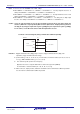
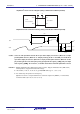
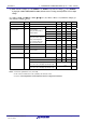
Classification of A/D converter characteristics
Input channel
Reference Voltage
Reference voltage (+) =
AV
REFP
Reference voltage (−) =
AV
REFM
Reference voltage (+) = V
DD
Reference voltage (−) = V
SS
Reference voltage (+) = V
BGR
Reference voltage (−) =
AV
REFM
ANI0 to ANI14
Refer to 3.6.1 (1). Refer to 3.6.1 (3). Refer to 3.6.1 (4).
ANI16 to ANI26
Refer to 3.6.1 (2).
Internal reference voltage
Temperature sensor output
voltage
Refer to 3.6.1 (1).
−
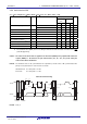
(1) When reference voltage (+) = AVREFP/ANI0 (ADREFP1 = 0, ADREFP0 = 1), reference voltage (−) =
AVREFM/ANI1 (ADREFM = 1), target pin : ANI2 to ANI14, internal reference voltage, and temperature
sensor output voltage
(T
A = −40 to +105°C, 2.4 V ≤ AVREFP ≤ VDD ≤ 5.5 V, VSS = 0 V, Reference voltage (+) = AVREFP, Reference
voltage (−) = AVREFM = 0 V)
Parameter Symbol Conditions MIN. TYP. MAX. Unit
Resolution RES 8 10 bit
Overall error
Note 1
AINL 10-bit resolution
AV
REFP = VDD
Note 3
2.4 V ≤ AV
REFP ≤ 5.5 V 1.2 ±3.5 LSB
Conversion time tCONV 10-bit resolution
Target pin: ANI2 to ANI14
3.6 V ≤ VDD ≤ 5.5 V 2.125 39
μ
s
2.7 V ≤ VDD ≤ 5.5 V
3.1875 39
μ
s
2.4 V ≤ VDD ≤ 5.5 V
17 39
μ
s
10-bit resolution
Target pin: Internal reference
voltage, and temperature
sensor output voltage (HS
(high-speed main) mode)
3.6 V ≤ V
DD ≤ 5.5 V 2.375 39
μ
s
2.7 V ≤ VDD ≤ 5.5 V
3.5625 39
μ
s
2.4 V ≤ VDD ≤ 5.5 V
17 39
μ
s
Zero-scale error
Notes 1, 2
E
ZS
10-bit resolution
AV
REFP = VDD
Note 3
2.4 V ≤ AV
REFP ≤ 5.5
V
±0.25 %FSR
Full-scale error
Notes 1, 2
E
FS
10-bit resolution
AV
REFP = VDD
Note 3
2.4 V ≤ AV
REFP ≤ 5.5
V
±0.25 %FSR
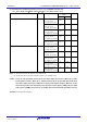
Integral linearity error
Note 1
ILE 10-bit resolution
AVREFP = VDD
Note 3
2.4 V ≤ AV
REFP ≤ 5.5
V
±2.5 LSB
Differential linearity error
Note 1
DLE 10-bit resolution
AVREFP = VDD
Note 3
2.4 V ≤ AV
REFP ≤ 5.5
V
±1.5 LSB
Analog input voltage VAIN ANI2 to ANI14 0 AVREFP V
Internal reference voltage output
(2.4 V ≤ V
DD ≤ 5.5 V, HS (high-speed main) mode)
V
BGR
Note 4
V
Temperature sensor output voltage
(2.4 V ≤ V
DD ≤ 5.5 V, HS (high-speed main) mode)
V
TMPS25
Note 4
V
(Notes are listed on the next page.)