
Datasheet


RL78/G13 3. ELECTRICAL SPECIFICATIONS (G: T
A = -40 to +105°C)
Page 166 of 194R01DS0131EJ0310 Rev.3.10
Nov 15, 2013
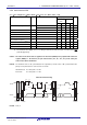
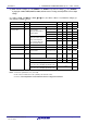
3.5.2 Serial interface IICA
(TA = −40 to +105°C, 2.4 V ≤ EVDD0 = EVDD1 ≤ VDD ≤ 5.5 V, VSS = EVSS0 = EVSS1 = 0 V)
Parameter Symbol Conditions HS (high-speed main) Mode Unit
Standard
Mode
Fast Mode
MIN. MAX. MIN. MAX.
SCLA0 clock frequency fSCL Fast mode: fCLK ≥ 3.5 MHz − − 0 400 kHz
Standard mode: fCLK ≥ 1 MHz 0 100 − − kHz
Setup time of restart condition tSU:STA 4.7 0.6
μ
s
Hold time
Note 1
t
HD:STA 4.0 0.6
μ
s
Hold time when SCLA0 = “L” tLOW 4.7 1.3
μ
s
Hold time when SCLA0 = “H” tHIGH 4.0 0.6
μ
s
Data setup time (reception) tSU:DAT 250 100 ns
Data hold time (transmission)
Note 2
t
HD:DAT 0 3.45 0 0.9
μ
s
Setup time of stop condition tSU:STO 4.0 0.6
μ
s
Bus-free time tBUF 4.7 1.3
μ
s
Notes 1. The first clock pulse is generated after this period when the start/restart condition is detected.
2. The maximum value (MAX.) of t
HD:DAT is during normal transfer and a wait state is inserted in the ACK
(acknowledge) timing.
Caution The values in the above table are applied even when bit 2 (PIOR2) in the peripheral I/O redirection
register (PIOR) is 1. At this time, the pin characteristics (I
OH1, IOL1, VOH1, VOL1) must satisfy the
values in the redirect destination.
Remark The maximum value of Cb (communication line capacitance) and the value of Rb (communication line
pull-up resistor) at that time in each mode are as follows.
Standard mode: C
b = 400 pF, Rb = 2.7 kΩ
Fast mode: C
b = 320 pF, Rb = 1.1 kΩ
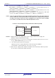
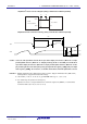
IICA serial transfer timing
t
R
t
BUF
t
F
t
LOW
t
HIGH
t
HD:STA
Stop
condition
Start
condition
Restart
condition
Stop
condition
t
SU:DAT
t
SU:STA
t
SU:STO
t
HD:STA
t
HD:DAT
SCLAn
SDAAn
Remark n = 0, 1