
Datasheet


Section 16 I2C Bus Interface 2 (IIC2)
R01UH0310EJ0500 Rev. 5.00 Page 957 of 1384
Sep 25, 2012
H8S/2426, H8S/2426R, H8S/2424 Group
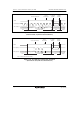
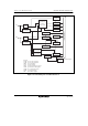
Vcc Vcc
SCL in
SCL out
SCL
SDA in
SDA out
SDA
SCL
(Master)
(Slave 1)
(Slave 2)
SDA
SCL in
SCL out
SCL
SDA in
SDA out
SDA
SCL in
SCL out
SCL
SDA in
SDA out
SDA
Figure 16.2 External Circuit Connections of I/O Pins
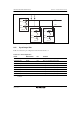
16.2 Input/Output Pins
Table 16.1 shows the pin configuration of the I
2
C bus interface 2.
Table 16.1 Pin Configuration
Name Abbreviation I/O Function
Serial clock pin SCL0 I/O IIC2_0 serial clock input/output
Serial data pin SDA0 I/O IIC2_0 serial data input/output
Serial clock pin SCL1 I/O IIC2_1 serial clock input/output
Serial data pin SDA1 I/O IIC2_1 serial data input/output
Serial clock pin SCL2 I/O IIC2_2 serial clock input/output
Serial data pin SDA2 I/O IIC2_2 serial data input/output
Serial clock pin SCL3 I/O IIC2_3 serial clock input/output
Serial data pin SDA3 I/O IIC2_3 serial data input/output
Note: The pin symbols are represented as SCL and SDA; channel numbers are omitted in this
manual.