
Datasheet

Section 15 Serial Communication Interface (SCI, IrDA)
R01UH0310EJ0500 Rev. 5.00 Page 879 of 1384
Sep 25, 2012
H8S/2426, H8S/2426R, H8S/2424 Group
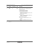
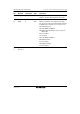
Bit Bit Name Initial Value R/W Description
2 TEIE 0 R/W Transmit End Interrupt Enable
Write 0 to this bit in Smart Card interface mode.
1
0
CKE1
CKE0
0
0
R/W
R/W
Clock Enable 1 and 0
Enables or disables clock output from the SCK
pin. The clock output can be dynamically switched
in GSM mode. For details, refer to section 15.7.8,
Clock Output Control.
When the GM bit in SMR is 0:
00: Output disabled (SCK pin can be used as an
I/O port pin)
01: Clock output
1x: Reserved
When the GM bit in SMR is 1:
00: Output fixed low
01: Clock output
10: Output fixed high
11: Clock output
[Legend]
x: Don't care