
Datasheet

Section 15 Serial Communication Interface (SCI, IrDA)
R01UH0310EJ0500 Rev. 5.00 Page 877 of 1384
Sep 25, 2012
H8S/2426, H8S/2426R, H8S/2424 Group
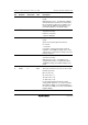
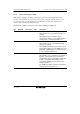
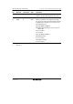
Bit Bit Name Initial Value R/W Description
1
0
CKE1
CKE0
0
0
R/W
R/W
Clock Enable 1 and 0
Selects the clock source and SCK pin function.
Asynchronous mode
00: On-chip baud rate generator
SCK pin functions as I/O port
01: On-chip baud rate generator
(Outputs a clock of the same frequency as the
bit rate from the SCK pin.)
1x: External clock
(Inputs a clock with a frequency 16 times the
bit rate from the SCK pin.)
Clocked synchronous mode
0x: Internal clock (SCK pin functions as clock
output)
1x: External clock (SCK pin functions as clock
input)
[Legend]
x: Don't care