
Datasheet

Section 15 Serial Communication Interface (SCI, IrDA)
R01UH0310EJ0500 Rev. 5.00 Page 873 of 1384
Sep 25, 2012
H8S/2426, H8S/2426R, H8S/2424 Group
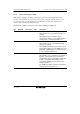
Smart Card Interface Mode (When SMIF bit in SCMR is 1)
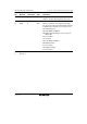
Bit Bit Name Initial Value R/W Description
7 GM 0 R/W GSM Mode
When this bit is set to 1, the SCI operates in GSM
mode. In GSM mode, the timing of the TEND
setting is advanced by 11.0 etu (Elementary Time
Unit: the time for transfer of 1 bit), and clock
output control mode addition is performed. For
details, refer to section 15.7.8, Clock Output
Control.
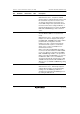
6 BLK 0 R/W When this bit is set to 1, the SCI operates in block
transfer mode. For details on block transfer mode,
refer to section 15.7.3, Block Transfer Mode.
5 PE 0 R/W Parity Enable (enabled only in asynchronous
mode)
When this bit is set to 1, the parity bit is added to
transmit data before transmission, and the parity
bit is checked in reception. In Smart Card interface
mode, this bit must be set to 1.
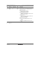
4 O/E 0 R/W Parity Mode (enabled only when the PE bit is 1 in
asynchronous mode)
0: Selects even parity.
1: Selects odd parity.
For details on setting this bit in Smart Card
interface mode, refer to section 15.7.2, Data
Format (Except for Block Transfer Mode).