
Datasheet


Section 15 Serial Communication Interface (SCI, IrDA)
Page 868 of 1384 R01UH0310EJ0500 Rev. 5.00
Sep 25, 2012
H8S/2426, H8S/2426R, H8S/2424 Group
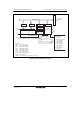
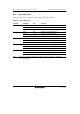
15.2 Input/Output Pins
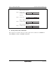
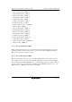
Table 15.1 shows the pin configuration of the serial communication interface.
Table 15.1 Pin Configuration
Channel Pin Name
*
I/O Function
SCK0 I/O Channel 0 clock input/output
RxD0/IrRxD Input Channel 0 receive data input (normal/IrDA)
0
TxD0/IrTxD Output Channel 0 transmit data output (normal/IrDA)
SCK1 I/O Channel 1 clock input/output
RxD1 Input Channel 1 receive data input
1
TxD1 Output Channel 1 transmit data output
SCK2 I/O Channel 2 clock input/output
RxD2 Input Channel 2 receive data input
2
TxD2 Output Channel 2 transmit data output
SCK3 I/O Channel 3 clock input/output
RxD3 Input Channel 3 receive data input
3
TxD3 Output Channel 3 transmit data output
SCK4 I/O Channel 4 clock input/output
RxD4 Input Channel 4 receive data input
4
TxD4 Output Channel 4 transmit data output
Note: * Pin names SCK, RxD, and TxD are used in the text for all channels, omitting the
channel designation.