
Datasheet

Section 12 Programmable Pulse Generator (PPG)
R01UH0310EJ0500 Rev. 5.00 Page 823 of 1384
Sep 25, 2012
H8S/2426, H8S/2426R, H8S/2424 Group
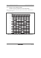
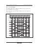
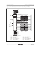
1. Set up the TPU channel to be used as the output trigger channel so that TGRA and TGRB are
output compare registers. Set the trigger period in TGRB and the non-overlap margin in
TGRA, and set the counter to be cleared by compare match B. Set the TGIEA bit in TIER to 1
to enable the TGIA interrupt.
2. Write H'FF in P1DDR and NDERH, and set the G3CMS1, G3CMS0, G2CMS1, and G2CMS0
bits in PCR to select compare match in the TPU channel set up in the previous step to be the
output trigger. Set the G3NOV and G2NOV bits in PMR to 1 to select non-overlapping output.
Write output data H'95 in NDRH.
3. The timer counter in the TPU channel starts. When a compare match with TGRB occurs,
outputs change from 1 to 0. When a compare match with TGRA occurs, outputs change from 0
to 1 (the change from 0 to 1 is delayed by the value set in TGRA). The TGIA interrupt
handling routine writes the next output data (H'65) in NDRH.
4. Four-phase complementary non-overlapping pulse output can be obtained subsequently by
writing H'59, H'56, H'95... at successive TGIA interrupts.
If the DTC or DMAC is set for activation by the TGIA interrupt, pulse output can be obtained
without imposing a load on the CPU.