
Datasheet

Section 12 Programmable Pulse Generator (PPG)
R01UH0310EJ0500 Rev. 5.00 Page 817 of 1384
Sep 25, 2012
H8S/2426, H8S/2426R, H8S/2424 Group
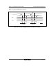
12.4.2 Sample Setup Procedure for Normal Pulse Output
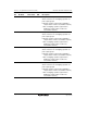
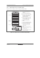
Figure 12.4 shows a sample procedure for setting up normal pulse output.
Select TGR functions
[1]
Set TGRA value
Set counting operation
Select interrupt request
Set initial output data
Enable pulse output
Select output trigger
Set next pulse
output data
Start counter
Set next pulse
output data
Normal PPG output
No
Yes
TPU setup
Port and
PPG setup
TPU setup
[2]
[3]
[4]
[5]
[6]
[7]
[8]
[9]
[10]
Compare match?
[1] Set TIOR to make TGRA an output
compare register (with output
disabled).
[2] Set the PPG output trigger period.
[3] Select the counter clock source with
bits TPSC2 to TPSC0 in TCR.
Select the counter clear source with
bits CCLR2 to CCLR0.
[4] Enable the TGIA interrupt in TIER.
The DTC or DMAC can also be set
up to transfer data to NDR.
[5] Set the initial output values in
PODR.
[6] Set the DDR and NDER bits for the
pins to be used for pulse output to 1.
[7] Select the TPU compare match
event to be used as the output
trigger in PCR.
[8] Set the next pulse output values in
NDR.
[9] Set the CST bit in TSTR to 1 to start
the TCNT counter.
[10] At each TGIA interrupt, set the next
output values in NDR.
Figure 12.4 Setup Procedure for Normal Pulse Output (Example)