
Datasheet

Section 12 Programmable Pulse Generator (PPG)
R01UH0310EJ0500 Rev. 5.00 Page 815 of 1384
Sep 25, 2012
H8S/2426, H8S/2426R, H8S/2424 Group
12.4 Operation
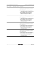
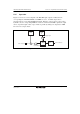
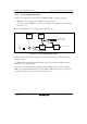
Figure 12.2 shows an overview diagram of the PPG. PPG pulse output is enabled when the
corresponding bits in P1DDR, P2DDR, and NDER are set to 1. An initial output value is
determined by its corresponding PODR initial setting. When the compare match event specified
by PCR occurs, the corresponding NDR bit contents are transferred to PODR to update the output
values. Sequential output of data of up to 16 bits is possible by writing new output data to NDR
before the next compare match.
Output trigger signal
Pulse output pin
Internal data bus
Normal output/inverted output
C
PODRQD
NDER
Q
NDRQ D
DDR
Figure 12.2 Overview Diagram of PPG