
Datasheet

Section 11 16-Bit Timer Pulse Unit (TPU)
R01UH0310EJ0500 Rev. 5.00 Page 799 of 1384
Sep 25, 2012
H8S/2426, H8S/2426R, H8S/2424 Group
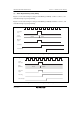
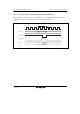
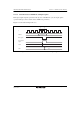
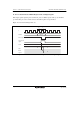
11.10.9 Contention between TGR Write and Input Capture
If the input capture signal is generated in the T
2
state of a TGR write cycle, the input capture
operation takes precedence and the write to TGR is not performed.
Figure 11.51 shows the timing in this case.
Input capture
signal
Write signal
Address
φ
TCNT
TGR write cycle
T
1
T
2
M
TGR
M
TGR address
Figure 11.51 Contention between TGR Write and Input Capture