
Datasheet

Section 11 16-Bit Timer Pulse Unit (TPU)
Page 798 of 1384 R01UH0310EJ0500 Rev. 5.00
Sep 25, 2012
H8S/2426, H8S/2426R, H8S/2424 Group
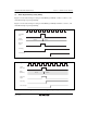
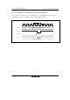
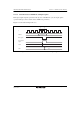
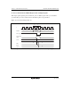
11.10.8 Contention between TGR Read and Input Capture
If the input capture signal is generated in the T
1
state of a TGR read cycle, the data that is read will
be the data after input capture transfer.
Figure 11.50 shows the timing in this case.
Input capture
signal
Read signal
Address
φ
TGR address
TGR
TGR read cycle
T
1
T
2
M
Internal
data bus
X M
Figure 11.50 Contention between TGR Read and Input Capture