
Datasheet

Section 11 16-Bit Timer Pulse Unit (TPU)
Page 762 of 1384 R01UH0310EJ0500 Rev. 5.00
Sep 25, 2012
H8S/2426, H8S/2426R, H8S/2424 Group
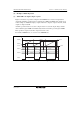
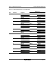
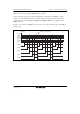
(b) When TGR is an input capture register
Figure 11.17 shows an operation example in which TGRA has been designated as an input
capture register, and buffer operation has been designated for TGRA and TGRC.
Counter clearing by TGRA input capture has been set for TCNT, and both rising and falling
edges have been selected as the TIOCA pin input capture input edge.
As buffer operation has been set, when the TCNT value is stored in TGRA upon occurrence of
input capture A, the value previously stored in TGRA is simultaneously transferred to TGRC.
TCNT value
H'09FB
H'0000
TGRC
Time
H'0532
TIOCA
TGRA
H'0F07H'0532
H'0F07
H'0532
H'0F07
H'09FB
Figure 11.17 Example of Buffer Operation (2)