
Datasheet

Section 11 16-Bit Timer Pulse Unit (TPU)
R01UH0310EJ0500 Rev. 5.00 Page 761 of 1384
Sep 25, 2012
H8S/2426, H8S/2426R, H8S/2424 Group
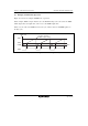
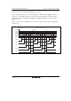
(2) Examples of Buffer Operation
(a) When TGR is an output compare register
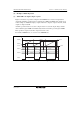
Figure 11.16 shows an operation example in which PWM mode 1 has been designated for
channel 0, and buffer operation has been designated for TGRA and TGRC. The settings used
in this example are TCNT clearing by compare match B, 1 output at compare match A, and 0
output at compare match B.
As buffer operation has been set, when compare match A occurs the output changes and the
value in buffer register TGRC is simultaneously transferred to timer general register TGRA.
This operation is repeated each time compare match A occurs.
For details on PWM modes, see section 11.4.5, PWM Modes.
TCNT value
TGRB_0
H'0000
TGRC_0
TGRA_0
H'0200 H'0520
TIOCA
H'0200
H'0450
H'0520
H'0450
TGRA_0
H'0450
H'0200
Transfer
Time
Figure 11.16 Example of Buffer Operation (1)