
Datasheet

Section 11 16-Bit Timer Pulse Unit (TPU)
R01UH0310EJ0500 Rev. 5.00 Page 759 of 1384
Sep 25, 2012
H8S/2426, H8S/2426R, H8S/2424 Group
11.4.3 Buffer Operation
Buffer operation, provided for channels 0, 3, 6, and 9, enables TGRC and TGRD to be used as
buffer registers.
Buffer operation differs depending on whether TGR has been designated as an input capture
register or a compare match register.
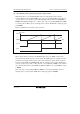
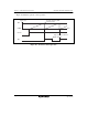
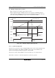
Table 11.29 shows the register combinations used in buffer operation.
Table 11.29 Register Combinations in Buffer Operation
Unit Channel Timer General Register Buffer Register
0 0 TGRA_0 TGRC_0
TGRB_0 TGRD_0
3 TGRA_3 TGRC_3
TGRB_3 TGRD_3
1 6 TGRA_6 TGRC_6
TGRB_6 TGRD_6
9 TGRA_9 TGRC_9
TGRB_9 TGRD_9
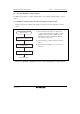
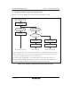
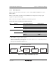
• When TGR is an output compare register
When a compare match occurs, the value in the buffer register for the corresponding channel is
transferred to the timer general register.
This operation is illustrated in figure 11.13.
Buffer register
Timer general
register
TCNTComparator
Compare match signal
Figure 11.13 Compare Match Buffer Operation