
Datasheet


Section 11 16-Bit Timer Pulse Unit (TPU)
R01UH0310EJ0500 Rev. 5.00 Page 729 of 1384
Sep 25, 2012
H8S/2426, H8S/2426R, H8S/2424 Group
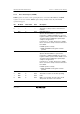
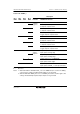
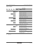
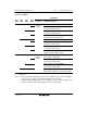
Table 11.18 TIORL_3
Description
Bit 7
IOD3
Bit 6
IOD2
Bit 5
IOD1
Bit 4
IOD0
TGRD_3
Function TIOCD3 Pin Function
0 0 0 0 Output disabled
1
Output
compare
register*
2
Initial output is 0 output
0 output at compare match
1 0 Initial output is 0 output
1 output at compare match
1 Initial output is 0 output
Toggle output at compare match
1 0 0 Output disabled
1 Initial output is 1 output
0 output at compare match
1 0 Initial output is 1 output
1 output at compare match
1 Initial output is 1 output
Toggle output at compare match
1 0 0 0 Capture input source is TIOCD3 pin
Input capture at rising edge
1 Capture input source is TIOCD3 pin
Input capture at falling edge
1 x
Input
capture
register*
2
Capture input source is TIOCD3 pin
Input capture at both edges
1 x x Capture input source is channel 4/count clock
Input capture at TCNT_4 count-up/count-down*
1
[Legend]
x: Don't care
Notes: 1. When bits TPSC2 to TPSC0 in TCR_4 are set to B'000 and φ/1 is used as the TCNT_4
count clock, this setting is invalid and input capture is not generated.
2. When the BFB bit in TMDR_3 is set to 1 and TGRD_3 is used as a buffer register, this
setting is invalid and input capture/output compare is not generated.