
Datasheet


Section 11 16-Bit Timer Pulse Unit (TPU)
Page 722 of 1384 R01UH0310EJ0500 Rev. 5.00
Sep 25, 2012
H8S/2426, H8S/2426R, H8S/2424 Group
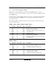
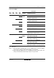
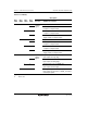
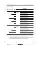
Table 11.12 MD3 to MD0
Bit 3
MD3*
1
Bit 2
MD2*
2
Bit 1
MD1
Bit 0
MD0 Description
0 0 0 0 Normal operation
1 Reserved
1 0 PWM mode 1
1 PWM mode 2
1 0 0 Phase counting mode 1
1 Phase counting mode 2
1 0 Phase counting mode 3
1 Phase counting mode 4
1 x x x ⎯
[Legend]
x: Don't care
Notes: 1. MD3 is a reserved bit. In a write, it should always be written with 0.
2. Phase counting mode cannot be set for channels 0 and 3. In this case, 0 should always
be written to MD2.