
Datasheet

Section 10 I/O Ports
Page 698 of 1384 R01UH0310EJ0500 Rev. 5.00
Sep 25, 2012
H8S/2426, H8S/2426R, H8S/2424 Group
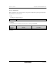
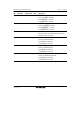
Bit Bit Name Initial Value R/W Description
4 TMRS 0 R/W TMR Pin Select
Selects the output pins of TMO1 and TMO0 and
input pins of TMCI1, TMCI0, TMRI1, and TMRI0.
0: [H8S/2426 Group, H8S/2426R Group]
P65/TMO1-A, P64/TMO0-A, P63/TMCI1-A,
P62/TMCI0-A, P61/TMRI1-A, and P60/TMRI0-A
are selected
[H8S/2424 Group]
P25/TMO1-A, P24/TMO0-A, P23/TMCI1-A,
P22/TMCI0-A, P21/TMRI1-A, and P20/TMRI0-A
are selected
1: P85/TMO1-B , P52/TMO0-B, P83/TMCI1-B,
P51/TMCI0-B, P81/TMRI1-B, and P50/TMRI0-B
are selected
3 to 1 ⎯ All 0 ⎯ Reserved
These bits are always read as 0. Only the initial
values should be written to these bits.
0 ⎯ 1 ⎯ Reserved
This bit is always read as 1. Only the initial value
should be written to this bit.
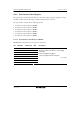
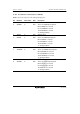
10.18.5 Port Function Control Register 4 (PFCR4)
PFCR4 switches the functions of the WAIT input pin, BREQ input pin, BACK output pin,
BREQO output pin, TxD4 output pin, RxD4 input pin, and SCK4 input/output pin.
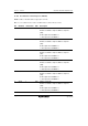
Bit Bit Name Initial Value R/W Description
7 WAITS 0 R/W WAIT Pin Select
Selects the WAIT input pin.
0: PF0/WAIT-A is selected
1: P25/WAIT-B is selected
6 BREQS 0 R/W BREQ Pin Select
Selects the BREQ input pin.
0: PG6/BREQ-A is selected
1: P51/BREQ-B is selected