
Datasheet

Section 10 I/O Ports
Page 696 of 1384 R01UH0310EJ0500 Rev. 5.00
Sep 25, 2012
H8S/2426, H8S/2426R, H8S/2424 Group
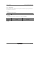
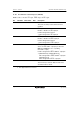
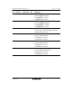
10.18.3 Port Function Control Register 2 (PFCR2)
PFCR2 enables or disables AS output, LWR output, and OE output.
Bit Bit Name Initial Value R/W Description
7 to 4 ⎯ All 0 ⎯ Reserved
These bits are always read as 0 and cannot be
modified.
3 ASOE 1 R/W AS Output Enable
Enables or disables the AS output pin.
0: PF6 is designated as I/O port
1: PF6 is designated as AS output pin
2 LWROE 1 R/W LWR Output Enable
Enables or disables the LWR output pin.
0: PF3 is designated as I/O port
1: PF3 is designated as LWR output pin
1 OES 1 R/W OE Output Select
Selects the OE*
2
/CKE*
1
output pin port when the
OEE bit in DRAMCR is set to 1 (enabling
OE*
2
/CKE*
1
output).
0: P35 is designated as OE-B*
2
/CKE-B*
1
output pin.
1: [H8S/2426 Group, H8S/2426R Group]
PH3 is designated as OE-A*
2
/CKE-A*
1
output pin.
[H8S/2424 Group]
PF0 is designated as OE-A*
2
output pin.
0 ⎯ 0 ⎯ Reserved
This bit is always read as 0. Only the initial value
should be written to this bit.
Notes: 1. Not supported in the H8S/2426 and H8S/2424 Groups.
2. Not supported in the 5-V version.