
Datasheet

Section 1 Overview
Page 42 of 1384 R01UH0310EJ0500 Rev. 5.00
Sep 25, 2012
H8S/2426, H8S/2426R, H8S/2424 Group
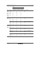
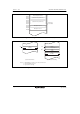
Pin No.
H8S/2426, H8S/2426R H8S/2424
Type Symbol PLQP0144KA-A PTLG0145JB-A
PLQP0120LA-A,
PLQP0120KA-A I/O Function
A/D
converter
AN15_1*
2
AN14_1*
2
128
127
D6
D7
⎯ Input Analog input pins.
AN13_1
AN12_1
126
125
D8
A8
104
103
Input Analog input pins.
AN11_1 to
AN8_1*
2
124 to 121 B7, C8, D9, A9 ⎯ Input Analog input pins.
AN7_0 to
AN0_0
120 to 113 B8, C9, B9, A10,
C10, B10, C11,
A11
102 to 95 Input Analog input pins.
ADTRG0-A
ADTRG0-B
ADTRG1
136
84
57
D4
J11
L8
112
69
48
Input Pin for input of an external trigger
to start A/D conversion.
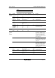
D/A
converter
DA3
DA2
126
125
D8
A8
104
103
Output Analog output pins.
A/D
converter,
D/A
converter
AV
CC
111 B11 93 Input Analog power-supply pin for the
A/D converter and D/A converter.
When the A/D converter and D/A
converter are not used, this pin
should be connected to the system
power supply (V
CC
).
AV
SS
129 A7 105 Input Ground pin for the A/D converter
and D/A converter. This pin should
be connected to the system power
supply (V
SS
).
Vref 112 B12 94 Input Reference voltage input pin for the
A/D converter and D/A converter.
When the A/D converter and D/A
converter are not used, this pin
should be connected to the system
power supply (V
CC
).
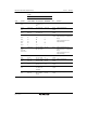
I/O ports P17 to
P10
49 to 42 L5, K6, K5, N4,
M5, L4, M4, N3
41 to 34 Input/
output
8-bit input/output pins.
P27 to
P20
58 to 51 K7, L8, N7, M7,
N6, M6, L7, L6
49 to 42 Input/
output
8-bit input/output pins.
P35 to
P30
137 to 142 A5, B4, C5, A4,
B3, C4
113 to 118 Input/
output
6-bit input/output pins.