
Datasheet

Section 10 I/O Ports
Page 680 of 1384 R01UH0310EJ0500 Rev. 5.00
Sep 25, 2012
H8S/2426, H8S/2426R, H8S/2424 Group
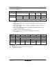
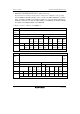
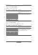
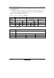
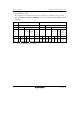
• PG3/CS3/RAS3*
2
/CAS*
1
The pin function is switched as shown below according to the combination of the operating
mode, bits RMTS2 to RMTS0 in DRAMCR of the bus controller, bit CS3E in PFCR0, and bit
PG3DDR.
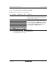
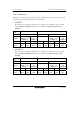
Operating
mode
1, 2, 4 3, 7
EXPE ⎯ 0 1
CS3E 0 1 ⎯ 0 1
RMTS2 to
RMTS0
⎯ Area 3 is in
normal space
Area 3 is
in DRAM
space
Areas 2 to 5
are in
synchronous
DRAM space
⎯ ⎯ Area 3 is in
normal space
Area 3 is
in DRAM
space
Areas 2 to 5
are in
synchronous
DRAM space
PG3DDR 0 1 0 1 ⎯ ⎯ 0 1 0 1 0 1 ⎯ ⎯
Pin function PG3
input
PG3
output
PG3
input
CS3
output
RAS3*
2
output
CAS*
1
output
PG3
input
PG3
output
PG3
input
PG3
output
PG3
input
CS3
output
RAS3*
2
output
CAS*
1
output
Notes: 1. Not supported in the H8S/2426 Group and H8S/2424 Group.
2. Not supported in the 5-V version.