
Datasheet

Section 10 I/O Ports
Page 676 of 1384 R01UH0310EJ0500 Rev. 5.00
Sep 25, 2012
H8S/2426, H8S/2426R, H8S/2424 Group
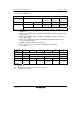
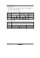
10.15.2 Port G Data Register (PGDR)
PGDR stores output data for the port G pins.
Bit Bit Name Initial Value R/W Description
7 ⎯ 0 ⎯ Reserved
This bit is always read as 0, and cannot be
modified.
6 PG6DR 0 R/W
5 PG5DR 0 R/W
4 PG4DR 0 R/W
3 PG3DR 0 R/W
2 PG2DR 0 R/W
1 PG1DR 0 R/W
0 PG0DR 0 R/W
Output data for a pin is stored when the pin
function is specified as a general purpose I/O.
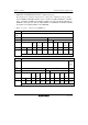
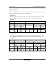
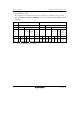
10.15.3 Port G Register (PORTG)
PORTG shows the pin states of port G. PORTG cannot be modified.
Bit Bit Name Initial Value R/W Description
7 ⎯ Undefined ⎯ Reserved
If this bit is read, it will return an undefined value.
6 PG6 ⎯* R
5 PG5 ⎯* R
4 PG4 ⎯* R
3 PG3 ⎯* R
2 PG2 ⎯* R
1 PG1 ⎯* R
0 PG0 ⎯* R
If this register is read while a PGDDR bit is set to 1,
the corresponding PGDR value is read. If this
register is read while a PGDDR bit is cleared to 0,
the corresponding pin state is read.
Note: * Determined by the states of pins PG6 to PG0.