
Datasheet

Section 10 I/O Ports
R01UH0310EJ0500 Rev. 5.00 Page 671 of 1384
Sep 25, 2012
H8S/2426, H8S/2426R, H8S/2424 Group
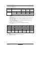
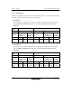
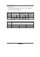
• Modes 3 and 7 (EXPE = 0)
WAITE ⎯
SSU settings (1) in table below (2) in table
below
(4) in table
below
(3) in table
below
PF0DDR 0 1 0*
5
0*
5
⎯
PF0 input PF0 output SCS0-C
input*
2
*
6
SCS0-C
I/O*
4
*
6
SCS0-C
output*
3
*
6
Pin function
ADTRG0-B input*
1
Notes: 1. ADTRG0-B input when the ADTRG0S bit in PFCR4 is 1, TRGS1 = TRGS0 = 0, and
EXTRGS = 1
2. When using as SCS0-C input, set SCS0S1 and SCS0S0 in PFCR5 to B'10 before other
register setting.
3. When using as SCS0-C output, set SCS0S1 and SCS0S0 in PFCR5 to B'10 before
other register setting.
4. When using as SCS0-C input/output, set SCS0S1 and SCS0S0 in PFCR5 to B'10
before other register setting.
5. PF0DDR = 0 when the SSU pin is used as input.
6. Do not set up for SSU unless SCS0S1 and SCS0S0 = B'10 in PFCR5.
Use as I/O port.
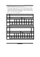
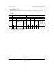
SSU settings (2) (1) (2) (4) (3) (1)
SSUMS 0 1
MSS 0 1 x
CSS1 x 0 1 x
CSS0 x 0 1 0 1 x
Pin state SCS input ⎯ SCS input Automatic
SCS I/O
SCS output ⎯
[Legend]
x: Don't care
⎯: Not used as the SSU pin (can be used as an I/O port).
Note: See tables 19.4 to 19.6.