
Datasheet


Section 10 I/O Ports
R01UH0310EJ0500 Rev. 5.00 Page 667 of 1384
Sep 25, 2012
H8S/2426, H8S/2426R, H8S/2424 Group
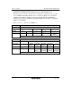
• PF1/UCAS*
7
/DQMU*
6
/IRQ14-A/SSCK0-C (H8S/2426 Group and H8S/2426R Group)
The pin function is switched as shown below according to the combination of the operating
mode, bit EXPE, bits MSS and SCKS in SSCRH and bit SSUMS in SSCRL of the SSU, bits
RMTS2 to RMTS0 in DRAMCR*
7
of the bus controller, bits SSCK0S1 and SSCK0S0 in
PFCR5, and bit PF1DDR.
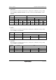
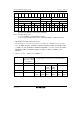
• Modes 1, 2, and 4 Modes 3 and 7 (EXPE = 1)
Areas 2 to 5 Any of areas 2 to 5 is
DRAM/synchronous
DRAM space
Areas 2 to 5 are all normal space
SSU settings ⎯ (1) in table below (2) in table
below
(3) in table
below
PF1DDR ⎯ 0 1 0*
4
⎯
UCAS*
7
output
DQMU*
6
output
PF1 input PF1 output SSCK0-C
input*
2
*
5
SSCK0-C
output*
3
*
5
Pin function
IRQ14-A interrupt input*
1
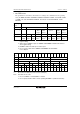
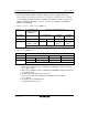
• Modes 3 and 7 (EXPE = 0)
Areas 2 to 5 ⎯
SSU settings (1) in table below (2) in table below (3) in table below
PF1DDR 0 1 0*
4
⎯
PF1 input PF1 output SSCK0-C input*
2
*
5
SSCK0-C output*
3
*
5
Pin function
IRQ14-A interrupt input*
1
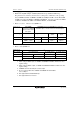
Notes: 1. IRQ14 input when the ITS14 bit in ITSR is 0.
2. When using as SSCK0-C input, set SSCK0S1 and SSCK0S0 in PFCR5 to B'10 before
other register setting.
3. When using as SSCK0-C output, set SSCK0S1 and SSCK0S0 in PFCR5 to B'10 before
other register setting.
4. PF1DDR = 0 when the SSU pin is used as input.
5. Do not set up for SSU unless SSCK0S1 and SSCK0S0 = B'10 in PFCR5.
Use as I/O port.
6. Not supported in the H8S/2426 Group.
7. Not supported in the 5-V version.