
Datasheet


Section 10 I/O Ports
R01UH0310EJ0500 Rev. 5.00 Page 639 of 1384
Sep 25, 2012
H8S/2426, H8S/2426R, H8S/2424 Group
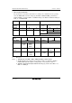
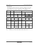
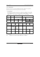
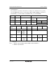
• PC6/A6/TIOCA11
The pin function is switched as shown below according to the combination of the operating
mode, bit EXPE, TPU channel 11 settings (by bits MD3 to MD0 in TMDR_11, bits IOA3 to
IOA0 in TIOR_11, and bits CCLR1 and CCLR0 in TCR_11), and bit PC6DDR.
Operating
mode
1, 2 4 3, 7 (EXPE = 1) 3, 7 (EXPE = 0)
TPU channel
11 settings
⎯ ⎯ (1) in table
below
(2) in table below
PC6DDR ⎯ 0 1 ⎯ 0 1
PC6 input PC6 output Pin function A6 output PC6 input A6 output TIOCA11
output
TIOCA11 input*
1
TPU channel 11
settings
(2) (1) (2) (1) (1) (2)
MD3 to MD0 B'0000, B'01xx B'001x B'0010 B'0011
IOA3 to IOA0 B'0000,
B'0100,
B'1xxx
B'0001 to
B'0011,
B'0101 to
B'0111
B'xx00 Other than B'xx00
CCLR1,
CCLR0
⎯ ⎯ ⎯ ⎯ Other than
B'01
B'01
Output function ⎯ Output
compare
output
⎯ PWM*
2
mode
1 output
PWM mode
2 output
⎯
[Legend]
x: Don't care
Notes: 1. TIOCA11 input when MD3 to MD0 = B'0000 or B'01xx and IOA3 = 1.
2. TIOCB11 output disabled.