
Datasheet


Section 1 Overview
Page 36 of 1384 R01UH0310EJ0500 Rev. 5.00
Sep 25, 2012
H8S/2426, H8S/2426R, H8S/2424 Group
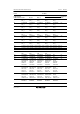
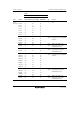
Pin No.
H8S/2426, H8S/2426R H8S/2424
Type Symbol PLQP0144KA-A PTLG0145JB-A
PLQP0120LA-A,
PLQP0120KA-A I/O Function
Bus
control
DQMU*
1
85 H12 ⎯ Output Upper data mask enable signal for
accessing the 16-bit continuous
synchronous DRAM space. Also
functions as the data mask enable
signal for accessing the 8-bit
continuous synchronous DRAM
space.
DQML*
1
86 H10 ⎯ Output Lower-data mask enable signal for
accessing the 16-bit continuous
synchronous DRAM interface
space.
RAS2*
3
RAS3*
3
RAS4*
2
*
3
RAS5*
2
*
3
109
110
35
36
A12
A13
L1
M1
91
92
⎯
⎯
Output Row address strobe signal for the
DRAM when the DRAM interface is
set. Row address strobe signal
when areas 2 to 5 are set as the
continuous DRAM space.
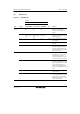
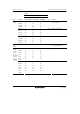
RAS*
1
109 A12 ⎯ Output Row address strobe signal for the
synchronous DRAM when the
synchronous DRAM interface is
set.
CAS*
1
110 A13 ⎯ Output Column address strobe signal for
the synchronous DRAM when the
synchronous DRAM interface is
set.
WE*
1
35 L1 ⎯ Output Write enable signal for the
synchronous DRAM when the
synchronous DRAM interface is
set.
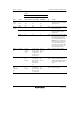
WAIT-A
WAIT-B
84
56
J11
N7
69
47
Input Requests insertion of a wait state
in the bus cycles when accessing
an external 3-state address space.
OE-A*
3
OE-B*
3
38
137
M2
A5
69
113
Output Output enable signal when
accessing the DRAM space.
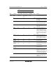
CKE-A*
1
CKE-B*
1
38
137
M2
A5
⎯
⎯
Output Clock enable signal when the
synchronous DRAM interface is
set.