
Datasheet

Section 10 I/O Ports
Page 620 of 1384 R01UH0310EJ0500 Rev. 5.00
Sep 25, 2012
H8S/2426, H8S/2426R, H8S/2424 Group
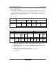
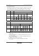
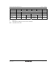
• PA3/A19/SCK4-B
The pin function is switched as shown below according to the combination of the operating
mode, bit EXPE, bit C/A in SMR_4 and bits CKE0 and CKE1 in SCR_4 of the SCI, bit A19E
in PFCR1, bit SCK4S in PFCR4, and bit PA3DDR.
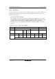
Operating
mode
1, 2 4
EXPE ⎯ ⎯
A19E ⎯ 0 1
CKE1 ⎯ 0 1 ⎯
C/A ⎯ 0 1 ⎯ ⎯
CKE0 ⎯ 0 1 ⎯ ⎯ ⎯
PA3DDR ⎯ 0 1 ⎯ ⎯ ⎯ 0 1
Pin function A19
output
PA3
input
PA3
output
SCK4-B
output*
SCK4-B
output*
SCK4-B
input*
PA3
input
A19
output
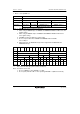
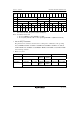
Operating
mode
3, 7
EXPE 0 1
A19E ⎯ 0 1
CKE1 0 1 0 1 ⎯
C/A 0 1 ⎯ 0 1 ⎯ ⎯
CKE0 0 1 ⎯ ⎯ 0 1 ⎯ ⎯ ⎯
PA3DDR 0 1 ⎯ ⎯ ⎯ 0 1 ⎯ ⎯ ⎯ 0 1
Pin function PA3
input
PA3
output
SCK4-B
output*
SCK4-B
output*
SCK4-B
input*
PA3
input
PA3
output
SCK4-B
output*
SCK4-B
output*
SCK4-B
input*
PA3
input
A19
output
Note: * When using as SCK4-B input/output, set SCK4S in PFCR4 to 1 before other register
setting.