
Datasheet


Section 1 Overview
R01UH0310EJ0500 Rev. 5.00 Page 35 of 1384
Sep 25, 2012
H8S/2426, H8S/2426R, H8S/2424 Group
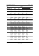
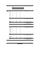
Pin No.
H8S/2426, H8S/2426R H8S/2424
Type Symbol PLQP0144KA-A PTLG0145JB-A
PLQP0120LA-A,
PLQP0120KA-A I/O Function
Bus
control
CS7 to
CS0
38 to 35,
110 to 107
M2, N2, M1, L1,
A13, A12, B13,
C12
29, 71, 70, 106,
92 to 89
Output Signals that select division areas 7
to 0 in the external address space
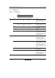
AS 90 G10 75 Output When this pin is low, it indicates
that address output on the address
bus is valid.
AH 90 G10 75 Output Signal for holding the address
when an address/data multiplexed
I/O space is being accessed.
RD 89 G12 74 Output When this pin is low, it indicates
that the external address space is
being read.
HWR 88 H11 73 Output Strobe signal indicating that an
external address space is to be
written to, and the upper half (D15
to D8) of the data bus is enabled.
Also functions as the write enable
signal for accessing the DRAM
space.
LWR 87 J13 72 Output Strobe signal indicating that an
external address space is to be
written to, and the lower half (D7
to
D0) of the data bus is enabled.
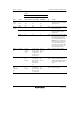
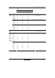
BREQ-A
BREQ-B
132
134
D5
B5
108
110
Input The external bus master requests
the bus to this LSI.
BREQO-A
BREQO-B
130
133
B6
A6
106
109
Output External bus request signal when
the internal bus master accesses
an external space in the external
bus release state.
BACK-A
BACK-B
131
135
C7
C6
107
111
Output Indicates the bus is released to the
external bus master.
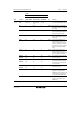
UCAS*
3
85 H12 70 Output Upper column address strobe
signal for accessing the 16-bit
DRAM space. Also functions as the
column address strobe signal for
accessing the 8-bit DRAM space.
LCAS*
3
86 H10 71 Output Lower column address strobe
signal for accessing the 16-bit
DRAM space.