
Datasheet

Section 10 I/O Ports
Page 616 of 1384 R01UH0310EJ0500 Rev. 5.00
Sep 25, 2012
H8S/2426, H8S/2426R, H8S/2424 Group
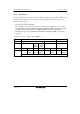
SSU
settings
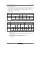
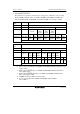
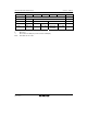
(1) (1) (3) (3) (2) (1) (2) (1) (1) (1) (1) (2) (1) (2) (2) (1) (2)
SSUMS 0 0 1*
1
BIDE 0 1*
2
0
MSS 0 1 0 1 0 1
TE 0 1 0 1 0 1 0 1 0 1 0 1
RE 0 1 0 1 1 0 1 1 0 1 0 1 0 1 1 0 1
Pin state ⎯ ⎯ SSI
output
SSI
output
SSI
input
⎯ SSI
input
⎯ ⎯ ⎯ ⎯ SSI
input
⎯ SSI
input
SSI
input
⎯ SSI
input
[Legend]
⎯: Not used as the SSU pin (can be used as an I/O port).
Notes: See tables 19.4 to 19.6.
1. Do not set BIDE to 1 when SSUMS = 1 in SSU.
2. Do not specify that TE = RE = 1 when operating with BIDE = 1 (bidirectional mode).
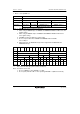
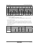
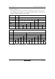
• PA5/A21/IRQ5-A/SSCK0-B
The pin function is switched as shown below according to the combination of the operating
mode, bit EXPE, bits MSS and SCKS in SSCRH and bit SSUMS in SSCRL of the SSU, bit
A21E in PFCR1, bits SSCK0S1 and SSCK0S0 in PFCR5, bit PA5DDR, and bit ITS5 in ITSR
of the interrupt controller
• Modes 1, 2, and 4
A21E 0 1
SSU settings (1) in table below (2) in table
below
(3) in table
below
⎯
PA5DDR 0 1 0*
4
⎯ 0 1
PA5 input PA5 output SSCK0-B
input*
2
*
5
SSCK0-B
output*
3
*
5
PA5 input A21 output Pin function
IRQ5-A interrupt input*
1