
Datasheet

Section 10 I/O Ports
Page 610 of 1384 R01UH0310EJ0500 Rev. 5.00
Sep 25, 2012
H8S/2426, H8S/2426R, H8S/2424 Group
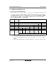
Bit Bit Name
Initial
Value R/W Description
• Mode 4 Modes 3 and 7 (EXPE = 1)
For pins PA6 to PA0, when the corresponding bit of A22E to
A16E is set to 1, setting a PADDR bit to 1 makes the
corresponding pin an address output, while clearing the bit to
0 makes the corresponding pin an input port. Clearing one of
bits A22E to A16E to 0 makes the corresponding pin an I/O
port, and its function can be switched with PADDR.
When A23E is 1, the PA7 pin functions as an address output
pin when the PA7DDR bit is set to 1, and as an input port
when the bit is cleared to 0.
When A23E is 0, operations differ between the H8S/2426
and H8S/2426R Groups and H8S/2424 Group.
[H8S/2426 Group and H8S/2426R Group]
When the PA7 pin is a general I/O port, the function can be
switched with PA7DDR.
[H8S/2424 Group]
When the CS output enable bit (CS7E) is 1, the PA7 pin
functions as a CS7 output pin when the PA7DDR bit is set to
1, and as an input port when the bit is cleared to 0. When the
CS output enable bit (CS7E) is 0 and the PA7 pin is a
general I/O port, the function can be switched with PA7DDR.
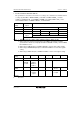
• Modes 3 and 7 (EXPE = 0)
Port A is an I/O port, and its pin functions can be switched
with PADDR.