
Datasheet


Section 1 Overview
Page 34 of 1384 R01UH0310EJ0500 Rev. 5.00
Sep 25, 2012
H8S/2426, H8S/2426R, H8S/2424 Group
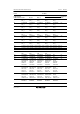
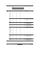
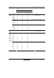
Pin No.
H8S/2426, H8S/2426R H8S/2424
Type Symbol PLQP0144KA-A PTLG0145JB-A
PLQP0120LA-A,
PLQP0120KA-A I/O Function
Operating
mode
control
MD2
MD1
MD0
1
144
143
B1
A2
A3
1
120
119
Input These pins set the operating mode.
These pins should not be changed
during operation.
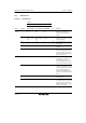
System
control
RES 92 G11 77 Input Reset pin. When this pin is driven
low, the chip is reset.
STBY 103 D13 88 Input When this pin is driven low, a
transition is made to hardware
standby mode.
EMLE 32 K1 30 Input On-chip emulator enable pin. When
the on-chip emulator is used, this
pin should be fixed high. At this
time, pins P53, PG4 to PG6, and
WDTOVF are used exclusively by
the on-chip emulator. Therefore,
the corresponding pin functions of
those pins are not available. When
the on-chip emulator is not used,
this pin should be fixed low.
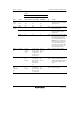
Address
bus
A23 to A0 31 to 26,
24 to 19,
17 to 11,
9 to 5
J3, K2, J1, K4,
H3, J2, J4, G3,
H2, G1, H4, G4,
F1, G2, F3, E4,
E1, F2, E3, D1,
D3, D2, C3, C1
29 to 23,
21 to 18,
16 to 9,
7 to 3
Output These pins output an address.
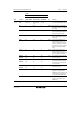
Data bus D15 to D0 80 to 73,
71,
69 to 63
K11, K12, L13,
L11, M12, L12,
N13, M13, N11,
M11, N10, L9,
M10, N9, K10,
L8
68 to 61,
59,
57 to 51
Input/
output
These pins constitute a
bidirectional data bus. When an
address/data multiplexed I/O space
is accessed, an address is also
output.
Address/
data
multiplexed
bus
AD15 to AD0 80 to 73,
71,
69 to 63
K11, K12, L13,
L11, M12, L12,
N13, M13, N11,
M10, N10, K10,
L10, M9, N9, K9
68 to 61,
59,
57 to 51
Input/
output
These pins output an address, and
input or output data.