
Datasheet

Section 10 I/O Ports
R01UH0310EJ0500 Rev. 5.00 Page 603 of 1384
Sep 25, 2012
H8S/2426, H8S/2426R, H8S/2424 Group
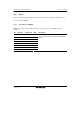
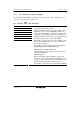
• P83/PO3-B/TIOCD3-B/TMCI1-B/RxD3
The pin function is switched as shown below according to the combination of the TPU channel
3 settings (by bits MD3 to MD0 in TMDR_3, bits IOD3 to IOD0 in TIORL_3, and bits
CCLR2 to CCLR0 in TCR_3), bit NDER3 in NDERL of the PPG, bit RE in SCR_3 of the
SCI, bits PPGS, TPUS, and TMRS in PFCR3, and bit P83DDR.
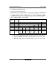
TPU channel 3
settings
(1) in table
below
(2) in table below
RE ⎯ 0 1
P83DDR ⎯ 0 1 ⎯
NDER3 ⎯ ⎯ 0 1 ⎯
P83 input P83 output PO3-B output*
3
RxD3 input TIOCD3-B
output*
4
TIOCD3-B input*
1
*
4
Pin function
TMCI1-B input*
2
*
5
Notes: 1. TIOCD3-B input when MD3 to MD0 = B'0000 and IOD3 to IOD0 = B'10xx.
2. When used as the external clock input pin for the TMR, its pin function should be
specified to the external clock input by the CKS2 to CKS0 bits in TCR_1 after the TMRS
bit in PFCR3 is set to 1.
3. When using as PO3-B output, set PPGS in PFCR3 to 1 before other register setting.
4. When using as TIOCD3-B input/output, set TPUS in PFCR3 to 1 before other register
setting.
5. When using as TMCI1-B input, set TMRS in PFCR3 to 1 before other register setting.
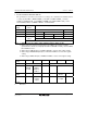
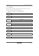
TPU channel 3
settings
(2) (1) (2) (2) (1) (2)
MD3 to MD0 B'0000 B'0010 B'0011
IOD3 to IOD0 B'0000,
B'0100,
B'1xxx
B'0001 to
B'0011,
B'0101 to
B'0111
⎯ B'xx00 Other than B'xx00
CCLR2 to
CCLR0
⎯ ⎯ ⎯ ⎯ Other than
B'110
B'110
Output function ⎯ Output
compare
output
⎯ ⎯ PWM mode
2 output
⎯
[Legend]
x: Don't care