
Datasheet


Section 1 Overview
R01UH0310EJ0500 Rev. 5.00 Page 33 of 1384
Sep 25, 2012
H8S/2426, H8S/2426R, H8S/2424 Group
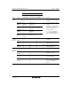
1.4.3 Pin Functions
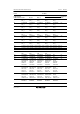
Table 1.5 Pin Functions
Pin No.
H8S/2426, H8S/2426R H8S/2424
Type Symbol PLQP0144KA-A PTLG0145JB-A
PLQP0120LA-A,
PLQP0120KA-A I/O Function
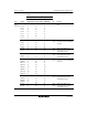
Power
supply
V
CC
4, 72, 98,
99
B2, N12, E11,
E13
2, 60, 83,
84
Input For connection to the power
supply. V
CC
pins should be
connected to the system power
supply.
V
SS
2, 10, 18,
25, 50, 70, 95,
102
A1, E2, F4, H1,
N5, M11, E10,
F11
8, 17, 22,
58, 80, 87
Input For connection to ground. V
SS
pins
should be connected to the system
power supply (0 V).
PLLV
CC
91 H13 76 Input Power supply pin for the on-chip
PLL oscillator.
PLLV
SS
93 G13 78 Input Ground pin for the on-chip PLL
oscillator.
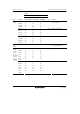
VCL 41 L3 33 Output This pin must not be connected to
the power supply and should be
connected to the V
SS
pin via a 0.1-
μF (recommended value) capacitor
(place it close to pin).
Clock XTAL 96 F12 81 Input For connection to a crystal
oscillator. See section 22, Clock
Pulse Generator, for typical
connection diagrams for a crystal
resonator and external clock input.
EXTAL 97 F13 82 Input For connection to a crystal
oscillator. The EXTAL pin can also
input an external clock. See section
22, Clock Pulse Generator, for
typical connection diagrams for a
crystal resonator and external clock
input.
φ 94 F10 79 Output Supplies the system clock to
external devices.
SDRAMφ*
1
36 M1 ⎯ Output When a synchronous DRAM is
connected, this pin is connected to
the CLK pin of the synchronous
DRAM. For details, refer to section
6, Bus Controller (BSC).