
Datasheet

Section 10 I/O Ports
R01UH0310EJ0500 Rev. 5.00 Page 599 of 1384
Sep 25, 2012
H8S/2426, H8S/2426R, H8S/2424 Group
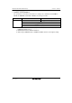
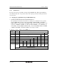
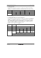
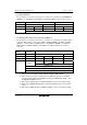
• P82/IRQ2-B/ETEND2
The pin function is switched as shown below according to the combination of bit ETENDE in
EDMDR_2 of the EXDMAC, bit P82DDR, and bit ITS2 in ITSR of the interrupt controller.
Operating mode 1, 2, 4 3, 7 (EXPE = 1) 3, 7 (EXPE = 0)
ETENDE 0 1 ⎯
P82DDR 0 1 ⎯ 0 1
P82 input P82 output ETEND2 output P82 input P82 output Pin function
IRQ2-B interrupt input*
Note: * IRQ2-B input when the ITS2 bit in ITSR is 1.
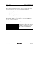
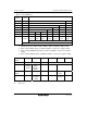
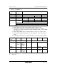
• P81/EDREQ3/IRQ1-B/TxD3/PO1-B/TIOCB3-B/TMRI1-B
The pin function is switched as shown below according to the combination of bit TE in SCR_3
of the SCI, TPU channel 3 settings (by bits MD3 to MD0 in TMDR_3, bits IOB3 to IOB0 in
TIORH_3, and bits CCLR2 to CCLR0 in TCR_3), bit NDER1 in NDERL of the PPG, bits
PPGS, TPUS, and TMRS in PFCR3, bit P81DDR, and bit ITS1 in ITSR of the interrupt
controller.
TPU channel 3
settings
(1) in table
below
(2) in table below
TE ⎯ 0 1
P81DDR ⎯ 0 1 1 ⎯
NDER1 ⎯ ⎯ 0 1 ⎯
P81 input P81 output PO1-B output*
4
TxD3 output TIOCB3-B
output*
5
TIOCB3-B input*
2
*
5
EDREQ3 input
IRQ1-B interrupt input*
1
Pin function
TMRI1-B input*
3
*
6
Notes: 1. IRQ1-B input when the ITS1 bit in ITSR is 1.
2. TIOCB3-B input when MD3 to MD0 = B'0000 and IOB3 to IOB0 = B'10xx.
3. When used as the counter reset input pin for the TMR, the external reset should be
selected using the CCLR1 and CCLR0 bits in TCR_1 and TMRIS bit in TCCR_1 after
the TMRS bit in PFCR3 is set to 1.
4. When using as PO1-B output, set PPGS in PFCR3 to 1 before other register setting.
5. When using as TIOCB3-B input/output, set TPUS in PFCR3 to 1 before other register
setting.
6. When using as TMRI1-B input, set TMRS in PFCR3 to 1 before other register setting.