
Datasheet

Section 10 I/O Ports
Page 596 of 1384 R01UH0310EJ0500 Rev. 5.00
Sep 25, 2012
H8S/2426, H8S/2426R, H8S/2424 Group
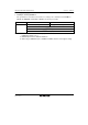
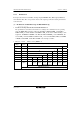
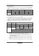
• Modes 3 and 7 (EXPE = 0)
TPU channel
4 settings
(1) in table
below
(2) in table below
OS3 to OS0 ⎯ All 0 Not all 0
AMS ⎯ ⎯ ⎯
CKE1 ⎯ 0 1 ⎯
C/A ⎯ 0 1 ⎯ ⎯
CKE0 ⎯ 0 1 ⎯ ⎯ ⎯
P85DDR ⎯ 0 1 1 ⎯ ⎯ ⎯ ⎯
NDER5 ⎯ ⎯ 0 1 ⎯ ⎯ ⎯ ⎯
P85
input
P85
output
PO5-B
output*
3
SCK3
output
SCK3
output
SCK3
input
TMO1-B
output*
5
TIOCB4-B
output*
4
TIOCB4-B input*
2
*
4
Pin function
IRQ5-B interrupt input*
1
Notes: 1. IRQ5-B input when the ITS5 bit in ITSR is 1.
2. TIOCB4-B input when MD3 to MD0 = B'0000 or B'01xx and IOB3 to IOB0 = B'10xx.
3. When using as PO5-B output, set PPGS in PFCR3 to 1 before other register setting.
4. When using as TIOCB4-B input/output, set TPUS in PFCR3 to 1 before other register
setting.
5. When using as TMO1-B output, set TMRS in PFCR3 to 1 before other register setting.
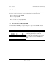
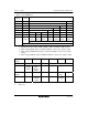
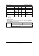
TPU channel 4
settings
(2) (1) (2) (2) (1) (2)
MD3 to MD0 B'0000, B'01xx B'0010 B'0011
IOB3 to IOB0 B'0000,
B'0100,
B'1xxx
B'0001 to
B'0011,
B'0101 to
B'0111
⎯ B'xx00 Other than B'xx00
CCLR1,
CCLR0
⎯ ⎯ ⎯ ⎯ Other than
B'10
B'10
Output function ⎯ Output
compare
output
⎯ ⎯ PWM mode
2 output
⎯
[Legend]
x: Don't care