
Datasheet


Section 10 I/O Ports
R01UH0310EJ0500 Rev. 5.00 Page 585 of 1384
Sep 25, 2012
H8S/2426, H8S/2426R, H8S/2424 Group
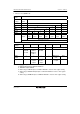
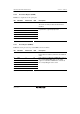
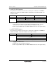
• Modes 3 and 7 (EXPE = 0)
BRLE ⎯
BREQOE ⎯
BREQOS ⎯
ICE 0 1
TPU channel 3
settings
(1) in table
below
(2) in table below ⎯
TE ⎯ 0 1 ⎯
P50DDR ⎯ 0 1 1 ⎯ ⎯
NDER0 ⎯ ⎯ 0 1 ⎯ ⎯
P50 input P50 output PO0-B
output*
6
TxD2
output
SDA3*
5
I/O
TIOCA3-B
output*
7
TIOCA3-B input*
1
*
7
IRQ0-A interrupt input*
2
Pin function
TMRI0-B input*
3
*
8
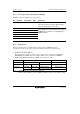
TPU channel 3
settings
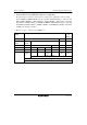
(2) (1) (2) (1) (1) (2)
MD3 to MD0 B'0000 B'001x B'0010 B'0011
IOA3 to IOA0 B'0000,
B'0100,
B'1xxx
B'0001 to
B'0011,
B'0101 to
B'0111
B'xx00 Other than
B'xx00
Other than B'xx00
CCLR2 to
CCLR0
⎯ ⎯ ⎯ ⎯ Other than
B'001
B'001
Output function ⎯ Output compare
output
⎯ PWM*
4
mode
1 output
PWM mode
2 output
⎯
Notes: 1. TIOCA3-B input when MD3 to MD0 = B'0000 and IOC3 to IOC0 = B'10xx.
2. IRQ0-A input when the ITS0 bit in ITSR is 0.
3. When used as the counter reset input pin for the TMR, the external reset should be selected
using the CCLR1 and CCLR0 bits in TCR_0 and TMRIS bit in TCCR_0 after the TMRS bit in
PFCR3 is set to 1.
4. TIOCB3-B output disabled.
5. NMOS open-drain output regardless of P50ODR.
6.
When using as PO0-B output, set PPGS in PFCR3 to 1 before other register setting.
7.
When using as TIOCA3-B input/output, set TPUS in PFCR3 to 1 before other register
setting.
8.
When using as TMRI0-B input, set TMRS in PFCR3 to 1 before other register setting.